Part 2 laid out the DRAM cell, one transistor and one capacitor (1T1C), and how a chip built from it is read, refreshed and addressed. The memory map had already ended on DRAM, the far end of the hierarchy, and gives the reasons none of the other memories it covers replaced it. This part asks what could follow that cell. A cell with no capacitor is one answer. A cell stacked in layers is another, and a ferroelectric capacitor that keeps its charge is a third. It starts with why the cell is hard to shrink and what refresh costs, then sets the candidates side by side, with results from labs kept apart from roadmaps. The other parts are on the series page.
Working Memory
Working Memory, Part 3: What Could Follow DRAM
Why the DRAM cell is hard to shrink, what refresh costs, and what capacitorless, stacked and ferroelectric cells trade, with labs kept apart from roadmaps.
On this page 23 sections
Why 1T1C is hard to shrink
The MRAM, ferroelectric and resistive families come in where they bear on that question, and each has its own part in the Beyond NAND series. Beyond NAND, Part 3 covers MRAM and looks at DRAM density from the MRAM side. Ferroelectric memory is in Beyond NAND, Part 4, and resistive memory is in Beyond NAND, Part 5.
This part is about what could replace the cell, and the array built from it. High Bandwidth Memory is a stack of separate dies and isn’t a new cell, while a monolithic 3D DRAM would be a different thing that Semiconductor Engineering says could later feed such a stack. So the stack belongs to Part 4 and its teardown stays in the Atlas, while the DRAM Timeline has the dies.
Results from devices and arrays carry one of four tags in the text, followed by a short source note. Lab means device or array data from a paper or a company’s own technical page. Reported means a trade-press account of a conference paper that this guide could not read. Roadmap means a company or industry statement of intent. Simulation means no silicon. Figures from analysts, standards bodies and reviews are attributed to their source, and where only an abstract or a company summary was read, the source note says so.
One transistor, one capacitor
Part 2 covers what a 1T1C cell is and how a read works. Cell area is counted in units of F², where F is the smallest feature the process can draw, and the memory map explains the unit and has the roadmap’s figures for the DRAM cell.
Samsung’s 2024 short course at the IEEE International Electron Devices Meeting (IEDM) tells the route to a smaller cell. In that account the unit cell shrank from 8F² to 6F² by using space that was empty in the layout, and reaching 4F² needs a further cut in the area the cell requires. That same course puts the cell array at 40% to 70% of the chip.
The 2022 International Roadmap for Devices and Systems (IRDS) names what stands in the way. One challenge is vertical transistor structures, and the other is high-k dielectrics, materials with a high dielectric constant (k), that raise capacitance per area while keeping leakage low. It adds that if the cost of scaling 2D DRAM becomes poor, scaling will stop and either 3D cell stacking or a new DRAM concept will be adopted. Both are discussed, it says, and there is no clear path beyond 2D DRAM (roadmap).
The capacitor runs out of room
Under the IRDS, the storage capacitor has to keep its capacitance as the cell shrinks, which leaves it less area to do so in. Cell capacitance is below 10fF in the DRAM generations TechInsights calls D1z and D1a, with the high-k dielectric thinned to 7nm or 6nm. Capacitance may fall to 5fF to 6fF at D1c, TechInsights adds, while the makers want to stay above 6fF to 7fF.
Its shape is a problem too. Samsung’s course lists four limits on conventional DRAM scaling, namely patterning, peripheral bandwidth, the cell transistor and the cell capacitor. A high aspect ratio in the cell capacitor raises the chance of bending and leakage, and bit-line capacitance rises significantly as the array tightens and the bit line and buried contact move closer.
A better dielectric is the materials answer. Equivalent oxide thickness (the oxide thickness that would give the same capacitance) must fall sharply for the capacitor in the IRDS roadmap. A ZrO2/Al2O3/ZrO2 stack serves 48nm to 30nm half-pitch, half the repeat distance of the densest lines. An ultra-high-k perovskite with a dielectric constant of 50 to 100 is expected to follow, and the capacitor shape changes from a cylinder to a pillar (roadmap). TechInsights puts the need for keeping capacitance above 7fF per cell while shrinking at a dielectric constant above 50, and names strontium titanate on ruthenium electrodes as a candidate whose equivalent oxide thickness might scale below 0.5nm.
Why 1T1C is hard to shrink
A 1T1C cell, with the sourced limits on its capacitor
Schematic, not to scale; the numbers beside it are TechInsights' figures
Figure 3.1 draws a 1T1C cell as a schematic, with the transistor under a capacitor and the limits the sources name: a tall capacitor, a thin dielectric and a bit line close by. It is not to scale and shows no aspect ratio. Around it sit TechInsights’ figures, each labeled with its source.
Shrinking is slowing
Every DRAM foundry has kept a 6F²-based cell design, and TechInsights’ design-rule chart covers Samsung, SK hynix and Micron from D2x through D1z. Micron’s shrink factor for the design rules sat at 0.75 to 0.85 for many years, rising to 0.92 at D1z, with Samsung and SK hynix above 0.92 at D1z too, which TechInsights reads as cells getting harder to shrink. Looking ahead, the shrink factor may stay above 0.9 for the next three generations of 6F² cells, D1a, D1b and D1c, and 10nm may be the last node for a 6F² cell, in TechInsights’ projection. A two-transistor, no-capacitor (2T0C) cell with indium gallium zinc oxide (IGZO) thin-film transistors, covered below, is a candidate for a later generation, it adds.
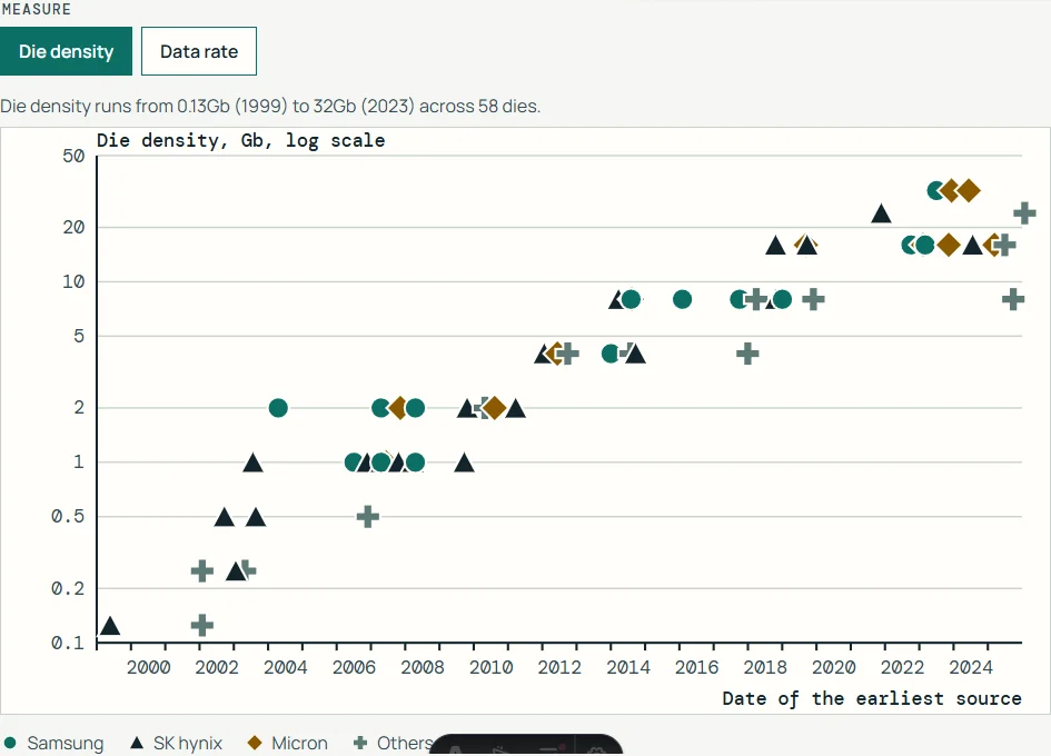
Density per die has still climbed. The earliest DDR die in the DRAM Timeline is SK hynix’s 128Mb DDR SDRAM from June 1999. SK hynix’s release is titled “HEI Has Released the Newly Standardized PC266A 128M DDR Synchronous DRAM for the First Time,” and HEI is SK hynix’s predecessor. That same timeline has Samsung’s 12nm-class 32Gb DDR5 part from September 2023, which Samsung announced on September 1, 2023 as the industry’s highest-capacity 12nm-class 32Gb DDR5 DRAM. Between those two rows the density per die rose 256 times, which is arithmetic on the two rows. It compares a 1999 die for which HEI released samples with a 2023 part that Samsung announced.
What refresh costs
A DRAM cell’s charge leaks away, so the bit has to be rewritten before it fades. imec says a smaller access transistor is a larger leakage path for the capacitor’s charge, which lowers retention time and requires more frequent refresh, with an impact on power consumption. A refresh is a row read with no column output, and Part 2 shows how it works.
The 32ms rule
Micron’s DDR5 16Gb die datasheet requires 8,192 refresh commands within 32ms from 0°C to 85°C, which is one command every 3.9µs. From 85°C to 95°C the window is 16ms and the interval 1.95µs. Part 2 covers what each command does and the 8,192-command arithmetic across DDR3, DDR4 and DDR5.
Refresh time grows with density
DRAM vendors refresh several rows with one command, to cut command traffic. A command takes longer as density rises, because more bits are handled in response to it (Stuecheli and colleagues, MICRO 2010). That time is the refresh cycle time, tRFC, defined in Part 2, which also shows that the growth is with density and not from one DDR generation to the next. Their table for DDR3 has tRFC rising from 90ns at 512Mb to 110ns at 1Gb, 160ns at 2Gb, 300ns at 4Gb and 350ns at 8Gb, against a refresh command interval, tREFI, of 7.8µs at 85°C and 3.9µs at 95°C.
Take tRFC over the interval and you have the share of time a chip is offline for refresh. The paper prints 1.3% for 512Mb and 4.5% for 8Gb at 85°C, and 9% for 8Gb at 95°C. Its 8Gb values match 350ns over 7.8µs and over 3.9µs, while the 512Mb value is a little above the 1.15% that 90ns over 7.8µs gives. The paper’s Figure 4(a) draws how long a read waits when it arrives just after a 300ns refresh of 4Gbit DRAM, against a typical closed-page access latency of 26ns.
Bhati and colleagues (IEEE Transactions on Computers, 2016) tabulate DDR4 at the 7.8µs interval, with 160ns for 2Gb, 260ns for 4Gb and 350ns for 8Gb. Kioxia puts the power needed to refresh cells as increasing in proportion to memory capacity. Part 2 gives DDR5 values from Micron’s DDR5 core datasheet (195ns at 8Gb to 410ns at 24Gb and 32Gb), while the figure below stays with DDR3 and DDR4.
What refresh costs
Refresh cycle time against density, and the time spent offline
tRFC for DDR3 and DDR4, time offline for DDR3, and a simulation strip
Figure 3.2 puts the refresh cycle time on the left against density on a log axis, with DDR3 and DDR4 as separate sets of points that are not joined. At 2Gb and 8Gb the two generations have the same tRFC, and at 4Gb DDR4 is lower. On the right is the share of time offline for DDR3, as the paper prints it. Under both panels, a strip shows a different kind of result: a simulation, which the next subsection explains.
Most refresh time protects a few weak cells
The RAIDR paper (Liu and colleagues, ISCA 2012) says the 64ms refresh window in the DRAM standards it was written against, which it calls the minimum refresh interval and which is twice DDR5’s 32ms, is needed by only a few weak cells. In a 32GB system, fewer than 1000 of more than 10¹¹ cells need an interval shorter than 256ms, using retention data from a 60nm process.
RAIDR groups DRAM rows into retention time bins and applies a different refresh rate to each bin, at a storage overhead of 1.25KB in the memory controller. In an 8-core system with 32GB of DRAM it cut refreshes by 74.6%. RAIDR’s authors evaluated it with an in-house x86 simulator with a cycle-accurate DRAM timing model. Energy per access fell by 8.3% below 85°C and by 16.1% from 85°C to 95°C, and system performance rose by 4.1% and 8.6% in the same two ranges. That is a simulation, not a measurement on silicon.
Capacitorless cells
The 2T0C cell stores its charge on a transistor gate and relies on the very low off-current of an oxide channel. The labs have shown it holding charge for seconds to hours, and those numbers cannot be read against a DRAM datasheet.
Two transistors, no capacitor
imec describes the 2T0C cell as one write transistor and one read transistor with no capacitor. Charge sits on the read transistor, and in imec’s 2020 cell the parasitic capacitance of the read transistor stores it. Samsung’s short course describes the same cell the same way, with a read transistor, a write transistor and no storage capacitor.
The channel is IGZO, an oxide semiconductor. imec says its wide bandgap gives a very low off-current, which relaxes the storage capacitance requirement, and that it deposits at a low temperature, so it fits in the back end of line, the metal and insulator layers above the transistors. That lets peripheral circuits sit under the array and opens the possibility of stacking cells.
Samsung shows an IGZO cell transistor with an off-current under 1fA per cell and a subthreshold swing, the gate voltage it takes to change the current below threshold tenfold, of 130mV per decade at 85°C (lab, Samsung’s IEDM 2023 result, shown in its course). Samsung also notes that the irregular cell pattern along the vertical direction makes process integration complex.
What the labs have shown
Every imec figure here comes from imec’s own pages, and all of the retention results below are lab results. imec presented at IEDM 2020 a 2T0C cell with retention above 400s, from an extracted off-current of 3×10⁻¹⁹A/µm, using 45nm gate-length transistors on 300mm wafers (lab, imec press release).
At IEDM 2021 it presented retention above 1,000s and endurance above 10¹¹ cycles after a gate-last integration with a buried oxygen tunnel, and a gate length scaled to 14nm that kept retention above 100s (lab, imec summary). imec’s overview of the cell adds a write time under 10ns for the same result (lab). imec said at the VLSI 2023 conference that patterning the active module of the 2T0C device by reactive ion etch instead of ion beam etch, which avoids the metal redeposition that ion beam etch causes and so cuts extrinsic leakage, improved the retention of IGZO 2T0C devices to more than 4.5 hours, with an off-current below 3×10⁻²¹A/µm, which imec calls the lowest value ever reported for 2T0C devices (lab, imec summary).
A Nature Communications paper (Liao and colleagues) demonstrates a vertical dual-gate IGZO 2T0C cell on a 4F² footprint with four-bit operation (lab). It defines retention as the time for the storage-node voltage to drop by 0.1V. The paper does not state the temperature for its Figure 4b values. The caption gives 350s and over 500s of retention with a 0.1V storage-node drop. Separately, the results text describing the same panel gives 470s for data ‘1’ and over 500s for data ‘0’.
A temperature sweep gives 90s at 85°C and 410s at 25°C. In its supplementary data, nine more cells exceed 100s for data ‘1’, with an average of 230s. It compares the 4F² footprint with a planar 2T0C of 20F² and cites that figure from a 2021 IEDM paper, and both footprints appear in the figure below.
These numbers are not the same kind as DDR5’s 32ms. DDR5’s 32ms is a rule for every cell in an array at up to 85°C. The imec figures come from summaries and a press release, not the papers, and those do not state at what temperature or by what failure criterion each was measured. The Nature Communications paper states its criterion and gives a temperature only for its sweep, and its 90s at 85°C, for one cell, is the one retention figure in this section stated at that temperature.
Capacitor kept, oxide transistor used
An oxide transistor is also being tried with the capacitor kept. Kioxia and Nanya’s oxide-semiconductor channel transistor DRAM (OCTRAM) is a 4F² cell with a vertical IGZO (InGaZnO) transistor built on top of a capacitor. Presented at IEDM 2024, its transistor has an on-current above 15µA and a leakage below 10⁻¹⁸A, and the cell retains data for over 100s (lab, Kioxia’s topic page).
Kioxia tested vertical gate-all-around IGZO transistors scaled below 25nm. After process optimization it estimates a time-dependent dielectric breakdown (TDDB) lifetime of more than 10 years (lab, topic page). Kioxia presented the result at the 2025 IEEE Symposium on VLSI Technology and Circuits. So an oxide transistor is being tried in two cell types, with and without a capacitor.
What is still open
Transistor lifetime and stacked integration are open. As noted above for Samsung’s cell, the IGZO pattern is irregular along the vertical direction. Take the lifetime figures with care. imec’s reliability model for IGZO transistors points to positive bias temperature instability (PBTI) as possibly the main degradation mechanism. It predicts a time to failure of about 20 days at operating conditions, improved to about one year by optimizing the gate dielectric, against a target of 5 years (model fitted to lab data; imec summary). Kioxia’s over 10 years is an estimate for a different mechanism, dielectric breakdown, in a different transistor, so the two figures are not the same lifetime.
Silicon gain cells are the contrast. A 2026 review says silicon-channel gain-cell embedded DRAM (eDRAM) still has limited retention, about 100µs in the 65nm macro it cites, and non-negligible refresh-related power as a mainstream memory, which is the gap oxide channels aim to close (lab, review).
imec has also built a 2T1C gain cell with two transistors and one metal-insulator-metal capacitor with a 9nm Al2O3 dielectric (lab, imec summary of its International Memory Workshop 2023 paper). Retention reached 130s, with a median off-current down to 1.5×10⁻¹⁹A/µm, and distinct voltage levels were still visible after 400s. Currents were summed in a 2x2 array, then in 4x2 arrays. imec presents it for analog in-memory computing as well as for DRAM. Summing currents in an array is the multiply-accumulate that Beyond NAND, Part 5 works through, where each cell’s current is a product and the shared line adds them.
Capacitorless cells
The 1T1C and 2T0C cells, and retention results on a log axis
Cells are schematics. Arrow: at least this value. Ring: silicon channel.
Figure 3.3 has two panels. On top are the two cells as schematics on the left and the two 2T0C footprints, to scale by area, on the right. Below is retention on a log axis in seconds, with the DDR5 refresh window as a reference line. In that lower panel the silicon gain-cell macro is the top row, drawn as a ring at the lowest value on the axis, and the vertical cell appears twice, at 85°C and at 25°C. Only those two rows have a stated temperature. An arrow marks a result given as a lower bound. Read plainly, oxide-channel cells have shown retention from tens of seconds at 85°C in one cell to hours in another, and the conditions for the hours aren’t stated. None of these cells is described as a memory product.
Stacking DRAM
Stacking results come in three kinds that are kept apart here. A first step changes the transistor and a second stacks layers, while a third stacks with an oxide channel.
Why DRAM did not stack
3D NAND stacked its cells in layers. A vertical capacitor makes DRAM layers very thick and hard to stack. Semiconductor Engineering reported in December 2024 that some efforts lay the capacitor on its side and others remove it, and that none was ready for production.
Samsung’s VLSI 2023 invited-paper abstract (in the symposium program) says shrinking DRAM far beyond the 10nm node raises process and reliability challenges, so DRAM may adopt vertical stacking of memory cells as 3D NAND did, adding layers to raise bit density and shrinking the transistor (roadmap; abstract only).
Step one: a vertical transistor
In the first step, the transistor changes. Samsung’s short course describes a shared-back-gate vertical channel transistor, cited to Samsung’s International Reliability Physics Symposium (IRPS) 2024 paper. Its back gate effect is 250mV/V, the threshold shift per volt on the back gate. Its variability is 40% lower than that of the buried-channel-array transistor in today’s cell, and its pass-gate effect (the disturbance from a neighboring gate) is below 50mV. The course does not say whether these figures were measured or simulated (lab or simulation, not stated). Wafer bonding lets the cell array sit on a separate peripheral circuit wafer, the course adds.
SK hynix’s CTO said at its VLSI 2025 plenary that SK hynix will apply a 4F² vertical gate platform and 3D DRAM at 10nm-level nodes and below (roadmap, SK hynix release). Separately, the release’s headline bullet says it is considering switching to the 4F² vertical gate platform from 10nm-level technology, a more cautious wording than the CTO’s. On cost, the CTO said the increase from the number of layers stacked can be solved by constant technological innovation.
SK hynix’s VLSI 2026 summary describes a 4F² vertical-gate DRAM array with the peripheral devices under the cell array, joined by fusion wafer bonding. A shared back gate trades some on-current and subthreshold swing for threshold control, and bit-line shielding reduces coupling noise and sensing failures. It shows working read and write operation and gives no retention or yield figure in the summary (lab, from a company summary).
Samsung’s version is reported by the trade press. A 10nm-class 4F² 16Gb prototype using a vertical channel transistor was shown at the IEEE International Solid-State Circuits Conference (ISSCC) 2026, according to The Elec. It uses wafer-to-wafer hybrid copper bonding, with a bond pitch of about 300nm and interconnects cut from 28.8 million to about 10 million. The Elec reports Samsung as saying the design could cut cell size by about 30% against 6F², and adds that the smaller cell could raise chip output per wafer by roughly 20%. Write tests ran from -25°C to 95°C, failed bits rose with temperature and stayed within repairable limits. Full verification for mass production isn’t complete yet (reported).
Semiconductor Engineering reported that Samsung announced efforts at the International Memory Workshop (IMW) 2024 on a 4F² vertical-channel cell that allows a capacitor at each word line and bit line intersection. It reported that the company aimed to complete this version in 2025 (reported, Semiconductor Engineering).
Step two: layers
Stacking is the second step. Samsung’s course compares its vertically stacked DRAM with the conventional cell: the channel body floats instead of being connected, and the transistor is double-gate or gate-all-around with a capacitor that lies on its side. Its roadmap slide puts the vertical channel transistors before stacked DRAM with silicon or IGZO channels. That slide is a roadmap and carries no product schedule. Samsung is working toward a 3D stacked DRAM with horizontal capacitors in the 2030 timeframe (roadmap, reported).
Three results give layer counts, and they are different kinds of evidence. SK hynix’s five-layer 3D DRAM at VLSI 2024 had a yield of 56.1%, about 561 working devices of roughly 1,000 on a test wafer, and behaved like 2D DRAM but less stably. That report also puts the layers needed for widespread use at 32 to 192 (reported; TrendForce, citing Business Korea).
Kioxia presented at IEDM 2025 a replacement process that swaps silicon nitride for IGZO to form horizontal oxide transistors (lab, Kioxia release, oxide transistors only). It verified the operation of transistors stacked in eight layers. They have an on-current above 30µA and an off-current below 10⁻¹⁸A. Refresh power can be reduced, Kioxia adds, thanks to the low off-current of oxide semiconductors.
Summarizing the symposium’s highlights, BigGo Finance has Samsung demonstrating a 16-layer vertically stacked DRAM at VLSI 2026, with gate-all-around cell transistors, horizontal capacitors, and the core and peripheral devices on a separate wafer bonded to the cell wafer (reported).
A fourth result has a larger layer count and is left off the figure, because it is not a memory. An imec and Ghent University paper in the Journal of Applied Physics grew stacks of up to 120 pairs, 241 sublayers, of 65nm silicon and 10nm Si0.8Ge0.2 on 300mm wafers for 3D DRAM, fully strained at the inner part of the wafers (lab, abstract only, as reproduced by Semiconductor Engineering). Misfit dislocations formed near the rim of the wafer. The abstract describes a crystal stack grown for 3D DRAM and does not say a memory cell was built in it.
Stacking DRAM
A stacked DRAM block as a schematic, and layer counts by evidence
Left: not to scale. Right: each bar is labeled with its evidence tag
Figure 3.4 draws a stacked block as a schematic, with horizontal capacitors, layers, a shared bit line and the peripheral circuits on a bonded wafer, and sets the three layer counts on one axis. Each bar carries its tag in its label, and two bars are reported and one is a lab result, with the note that its eight layers are oxide transistors only. A band marks the 32 to 192 layers the report says are needed, labeled as a stated need and not as a result. The largest count of stacked memory layers reported as built here is 16, reported, and the smallest count named as needed is 32.
Stacking with an oxide channel
Stacking cells with single-crystal silicon channels as in conventional DRAM raises manufacturing cost, in Kioxia’s account. imec’s reason for stacking a capacitorless cell is the oxide channel’s low deposition temperature, above. NEO Semiconductor’s press release proposes 1T1C and 3T0C 3D X-DRAM cells with IGZO channels on a modified 3D NAND process, so one of its two cells keeps a capacitor. It says technology computer-aided design (TCAD) simulations confirm 10ns read and write and retention of about 450s (the release says both “over” and “up to”). It expects proof-of-concept test chips in 2026 (simulation; no silicon shown).
What each candidate trades
Just one candidate in the matrix is new to this part: ferroelectric NVDRAM, short for nonvolatile DRAM.
Ferroelectric NVDRAM, in numbers
Micron’s NVDRAM is a ferroelectric memory with a DRAM-like cell at 4F², and Beyond NAND, Part 4 covers the 32Gb array and the physics behind it. Here it is a DRAM successor, and the numbers are the ones that part does not carry. All come from Micron’s own IEDM 2023 paper (lab, from a vendor paper).
Micron’s ferroelectric cell holds an effective 2Pr (the switched charge as Beyond NAND, Part 4 defines it) above 55µC/cm² at 1.5V while cycling to 10¹² cycles, with a peak of 64µC/cm². Figure 9 of the paper shows polarization against cycles, measured at 35°C. Its Figure 15a shows the zero and one distributions for NVDRAM die at 35°C. A representative yielding 32Gb die has zero fails, a bit error rate under 3×10⁻¹¹ across both decks (the two stacked layers of the die) and a read window of 750mV at -6.54 sigma. Separate distributions after 10¹⁰ endurance cycles at 95°C are shown with no window figure.
Micron also shows operation from -40°C to 95°C, and no fails on a 1Gb array after 100,000 row-hammer cycles, repeated activations meant to disturb neighboring rows. It extrapolates a positive read window at the 3×10⁻¹¹ bit error rate to 10 years of use. That extrapolation uses reliability data collected at 95°C and 1.5V and Micron’s internal lifetime model.
Refresh changes character. In Micron’s account, its NVDRAM repurposes the refresh command as a memory maintenance command that isn’t required when there is no activity. Maintenance overhead is about 20 times lower than DRAM refresh at 100% activity and about 150 times lower at 10% activity.
Speed is the trade. NVDRAM keeps the LPDDR5 command protocol, but its array timing is slower. In the paper’s IEDM 2023 handout, the figure labels give a row cycle time, tRC, of 185ns against 60ns for typical LPDDR5, while the text says only that longer array sensing and write-back raise the row-to-column delay tRCD and the precharge time tRP, and that the write recovery time tWR gets shorter.
Micron positions the part for capacity attached over Compute Express Link (CXL), since CXL lets a memory depart from strict DRAM timings, and says reduced refresh overhead lets designers consider capacities of 128Gb or more.
What Micron says about the others
Micron’s paper also says none of the studied technologies can directly replace DRAM from a product standpoint, given DRAM’s strict latency, power and bandwidth requirements. Resistive, phase-change and 3D XPoint memories have longer latencies that limit them to storage-class memory. Spin-transfer-torque (STT) and ferroelectric memories can achieve near-DRAM latencies, it says, but STT scalability and capacity are limited by high cell current and low sense margin in scaled cells. That is Micron’s view, from a paper that presents its own NVDRAM. Beyond NAND, Part 3 has the MRAM density figures and its speed section the timing of a standalone part, and Beyond NAND, Part 2 has the Optane latency.
Where each stands
Sorted by tag, the results in this part fall in four groups. Lab results cover the 2T0C and OCTRAM cells, SK hynix’s 4F² array, Micron’s NVDRAM, the eight oxide layers and the 120-pair crystal stack. Reported results are Samsung’s 4F² prototype and its 16 layers, and SK hynix’s five layers, all through the trade press. Samsung’s 2030 stacking target and its IMW 2024 aim are also trade-press reports.
Roadmap statements come from the IRDS, SK hynix’s 4F² and 3D plan and Samsung’s slide. Simulation results are NEO’s cells and the RAIDR refresh scheme. Samsung’s shared-back-gate transistor figures are the untagged result, for the reason given above. None of these is described as a DRAM replacement on sale. Memory and Storage for SI, Part 8 has the full sort across every memory family.
The matrix
The matrix holds five candidates: the 4F² vertical-channel cell, the stacked cell, the oxide-channel 2T0C, the oxide-channel cell with a capacitor and ferroelectric NVDRAM. Samsung’s description of its 4F² cell keeps the capacitor, and the SK hynix sources cited here do not say. Samsung’s course also lists three ferroelectric routes to 3D DRAM as candidates for later nodes: a ferroelectric RAM (FeRAM) cell with one transistor and one capacitor, a FeRAM with one transistor and several capacitors (1TnC), and a ferroelectric field-effect transistor (FeFET) cell it calls FeVRAM. Beyond NAND, Part 4 covers both device types. Those are proposals and are not in the matrix.
What each candidate trades
Five candidates against what the sources show for each
Shaded by evidence tag; not shown means no figure is given
Figure 3.5 sets each candidate against footprint, retention or refresh, speed and the path to more density. Cell shading is the evidence tag: lab, reported or roadmap. A cell without a figure reads “not shown” in the matrix. The stacked cell has no figure in three of its four columns. Most of the lab figures belong to the 2T0C cell, the OCTRAM cell and the ferroelectric cell. Two speeds are shown, and only the ferroelectric array’s is set against DRAM, where it is the slower one. Of the five, the 4F² vertical-channel cell looks the nearest step from today’s DRAM, since Samsung’s keeps the capacitor and both makers have put the cell on a roadmap or a prototype. It lacks a retention or speed figure, and that is the gap to watch. The oxide-channel and ferroelectric cells have figures, but each carries an open trade. Oxide transistor lifetime is unsettled, and the NVDRAM array is slower than LPDDR5.
Part 4 turns to High Bandwidth Memory, the stack of separate dies that this part set aside. It looks at why a stack’s bus is wide rather than fast, and why the chip edge limits bandwidth.
Sources
Primary is the original paper, standard or datasheet. Secondary is a review, a vendor summary or a news report. Measured is my own test data.
Show all 29 sources, 21 primary
- PrimaryHEI Has Released the Newly Standardized PC266A 128M DDR Synchronous DRAM for the First TimeSK hynix, 1999
- PrimaryStuecheli et al. 2010 Elastic Refresh: techniques to mitigate refresh penalties in high density memoryMICRO 2010 (University of Texas at Austin), 2010
- PrimaryLiu et al. 2012 RAIDR: Retention-aware intelligent DRAM refreshISCA 2012 (Carnegie Mellon, copy hosted by ETH Zurich), 2012
- PrimaryDRAM refresh mechanisms, penalties, and trade-offsIEEE Transactions on Computers (University of Maryland), 2016
- Primaryimec demonstrates capacitor-less IGZO-based DRAM cell with >400s retention time (IEDM 2020 press release)imec, 2020
- Primaryimec: Capacitor-less IGZO-based DRAM cell with excellent retention, endurance and gate length scaling (IEDM 2021 summary)imec, 2021
- PrimaryMicron DDR5 SDRAM: product core data sheetMicron Technology (copy hosted by Farnell), 2022
- Primaryimec: IGZO-based DRAM for energy and area-efficient analog in-memory computingimec, 2023
- PrimaryMicron 16Gb DDR5 SDRAM Die Rev A: data sheet addendumMicron Technology (copy hosted by Farnell; micron.com download is login-gated), 2023
- PrimaryRamaswamy et al. 2023 NVDRAM: A 32Gb dual layer 3D stacked non-volatile ferroelectric memory with near-DRAM performance (IEDM 2023 handout)Micron Technology (IEDM 2023 handout), 2023
- PrimarySamsung Electronics Unveils Industry’s Highest-Capacity 12nm-Class 32Gb DDR5 DRAM, Ideal for the AI EraSamsung, 2023
- PrimaryVLSI 2023 advance program (TFS1-1 Han et al., Samsung, Vertically Stacked DRAM abstract)2023 Symposium on VLSI Technology and Circuits (advance program), 2023
- PrimaryEvolution of Memory Technologies for Advanced Nodes via the 3rd DimensionIEDM 2024 short course, 2024
- PrimaryKioxia: Oxide-semiconductor Channel Transistor DRAM (OCTRAM) with 4F2 Architecture (IEDM 2024 topic page)Kioxia, 2024
- PrimaryEpitaxial Growth Of Up To 120 Si/SiGe Bilayers In View of 3D DRAM Applications (imec, Ghent Univ.)Semiconductor Engineering (abstract of Journal of Applied Physics paper), 2025
- PrimaryHigh-density three-dimensional integration of dynamic random-access memory using vertical dual-gate IGZO TFTsNature Communications, 2025
- PrimaryKioxia develops core technology for practical implementation of high-density, low-power 3D DRAM (release)Kioxia, 2025
- PrimaryKioxia: Time-dependent dielectric breakdown in sub-25nm gate-all-around vertical InGaZnO transistor for 4F2 DRAM (VLSI 2025 topic page)Kioxia, 2025
- PrimarySK hynix presents future DRAM technology roadmap at IEEE VLSI 2025SK hynix Newsroom, 2025
- Primary[Summary] Electrical characteristics of the 4F2 vertical gate (VG) DRAM integrated with bit-line shielding (BLS) and back gate (BG) transistorSK hynix Research (author Joodong Park, VLSI 2026 summary), 2026
- Primaryimec: Disrupting the DRAM roadmap with capacitor-less IGZO DRAM technologyimec
- SecondaryInternational Roadmap for Devices and Systems 2022 Edition: More MooreIEEE IRDS, 2022
- SecondaryBaby steps toward 3D DRAMSemiconductor Engineering, 2024
- SecondaryTrendForce: SK hynix 3D DRAM five-layer stacked yield at VLSI 2024TrendForce, 2024
- SecondaryNEO Semiconductor unveils 1T1C and 3T0C IGZO-based 3D X-DRAM technologyNEO Semiconductor (press release), 2025
- SecondaryOxide semiconductor gain cell-embedded memory: materials and integration strategies for next generation on-chip memoryCommunications Engineering (Nature Portfolio), 2026
- SecondarySamsung showcases new technologies for next-generation DRAMThe Elec, 2026
- SecondaryVLSI 2026 submissions top 1,000; highlights incl. Samsung 16-layer VS-DRAM and SK hynix 4F2 VG DRAMBigGo Finance, 2026
- SecondaryDRAM Scaling Trend and BeyondTechInsights