SSD Atlas is a 3D model of an M.2 NVMe SSD that opens from the board down to a single NAND cell. This is its build log, written at launch in September 2026, covering the design decisions that held up, the bugs that taught me something, and the rule about honesty that every figure in the app follows.
Engineering
How I Built the SSD Atlas, a 3D M.2 Map
The design decisions, bugs and honesty rules behind an interactive 3D reference for an M.2 NVMe SSD, from the board down to a single NAND cell.
On this page 14 sections
SSD Atlas has grown since, and as of November 1, 2026 it also takes apart an HBM stack and a DDR5 memory stick, and everything below describes the SSD the way I built it.
What SSD Atlas is
SSD Atlas is an interactive 3D reference for a generic M.2 2280 NVMe SSD. You orbit the board, click a part, and open it up, whether that part is the controller, DRAM, NAND, power management, a passive or the connector. It began on September 5, 2026 with a blank project and one question. What would make a datasheet term finally land somewhere physical?
What SSD Atlas is
You orbit the board, click a part, and open it
There are two halves, the app and its marketing page on this site, built separately and launched separately. The app first ran at ssd.eyesonflash.com, and it now lives at atlas.eyesonflash.com.
The stack
React, TypeScript and Vite make up the app, with the 3D scene built on three.js through React Three Fiber. A small Zustand store holds the current selection and camera requests, CSS handles the layout, and there is no backend.
The stack
The shell loads first, and the 3D viewer loads after it
Almost everything on screen is generated in code rather than loaded from a model file. The production build has no meshes or textures beyond the favicon, and comes to about 1.7MB in total. The 3D viewer is a lazy-loaded chunk of about 1.2MB (about 347kB gzipped), which loads after the shell at about 122kB gzipped so the navigation works before the scene finishes. If WebGL fails, the page falls back to the HTML navigation.
Before writing any of it, I studied Human Atlas, an interactive body atlas, for how it handles picking an object and showing what you picked, at desktop and phone sizes. That study is credited inside the app.
Depth without getting lost
Explore Inside is the core idea. Select a package and open it, and the parts around it fade while its interior takes over the board. Every depth is a node in one graph, and that graph drives the inspector, the breadcrumbs and the camera path.
Two rules make deep views usable. Wheel zoom never changes the semantic depth, so scrolling can’t skip you past a level. Escape, Back and the breadcrumbs always take you one level up, and Reset returns you to the default view.
Depth without getting lost
Every depth is a node in one graph
Take the controller. Its second view carried too many labels and ideas at once, and the fix was more levels, not fewer. It now has five steps, and each does one job:
| Level | View | What it answers |
|---|---|---|
| 1 | Package | The outside envelope |
| 2 | Wire-bond | How the die is connected |
| 3 | Architecture | The jobs: host, CPU, SRAM and NAND, with the flash translation layer running on the CPU |
| 4 | Floorplan | The area: mostly SRAM, with a small core complex |
| 5 | Mechanism | An SRAM macro or the CPU cores up close |
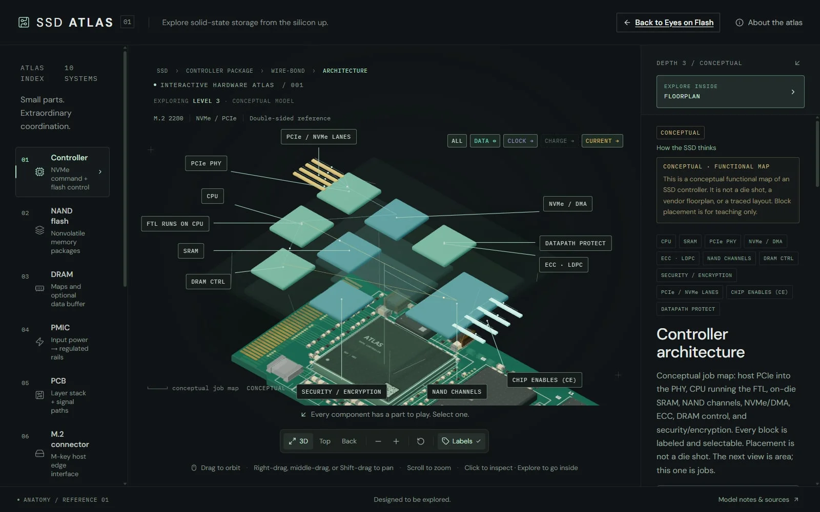
Jobs, area and mechanism are three different questions, and one view can’t answer all of them. NAND has its own path, running from package and wire-bond through die, plane, block and page to a charge-trap string. Its wire-bond step was missing at first, and I only noticed because the controller had one.
Honest geometry
A teaching model is only useful if it doesn’t lie. Every figure carries one of three classifications, verified, representative or conceptual. Verified covers the M.2 2280 outline, 0.50mm pitch and M-key slot, representative covers a NAND package envelope, and conceptual covers a functional map of the controller.
Honest geometry
Every figure says how far to trust it
A pre-launch audit caught two places where I had overclaimed. I had badged the connector as verified while its mesh draws 35 pads per face, and the standard describes 67 or 75 contact positions. Its PCB card also claimed a verified thickness that the evidence didn’t cover. Both were demoted to representative, and the About text now says plainly that the pads are a teaching mesh.
I also pulled a “Sources & assumptions” panel that showed “not yet reviewed” on some views. I decided a badge like that shouldn’t go live until the sources behind it were actually checked.
The bugs that taught me something
Of the six bugs below, only the first two stopped the page from working at all, a blank page and a crash. Behavior bugs in picking, depth and the camera made up most of the rest, plus some repeated text.
The bugs that taught me something
Six bugs, each with the fix that closed it
The page loaded and then went blank
My dev server had cached an empty stub of the viewer module, and the lazy import crashed, and clearing the build cache fixed it without touching the viewer.
The whole viewer crashed on one change
I had swapped the NAND wire-bond lines for 3D tubes that rebuilt their geometry every frame, and WebGL didn’t survive it. The wires went back to stable lines, built once.
Clicking one NAND package selected all four
The first click on a NAND package selected all four of them, which is fixed, so each package is now selected on its own.
Parts vanished in deep views
Components dropped out as you went deeper, and interiors could show through the board. Deep views now sit above the PCB, and the board fades consistently around them.
The model jumped when I started to rotate
Orbiting now pivots around the point you grabbed, and clicking a part never reframes the view.
Duplicate explanations
Several levels had reworded copies of the same “how to read this figure” text. Each level now has its own.
The marketing page
The landing page needed its own iteration. Its hero went from a CSS-drawn board to a spec-accurate M.2 2280 drawing, then to a photoreal still, back to a two-NAND drawing, and finally to a real capture of the running 3D app.
The marketing page
The hero went through five versions before the real app
Its component strip started with six cards and grew to ten, adding capacitors, resistors, a crystal and inductors. Alignment was the constant fight. A long line of text in one card pushed its image block down and everything under it with it, so every card now has a fixed-height slot for its icon and a reserved height for its copy. Both the NAND and DRAM icons were redrawn, as a stacked BGA and an isometric FBGA package.
I reverted two experiments, a set of landing-page callouts with a jump rail and a teaching cutaway of a NAND cell.
Launching it
Before launch I ran a gated audit of type check, lint, tests, build and a scan of the public output, all of which passed.
Launching it
Five checks passed before launch
There were 138 tests at that point, covering the anatomy graph, the connector layout and the accuracy classifications. It ended with a verdict of “ready to launch with minor issues”, and the minor issues were no deep links, a single board and a connector mesh that is illustrative. I deployed the app to Cloudflare Pages.
What I’d do next
At launch, deep links were the obvious gap. You couldn’t yet share a link to the inside of a specific package, and I wanted to. Since then the Atlas has gained deep links into specific parts.
What I’d do next
Deep links and a real connector closed gaps
Next on my list in September were a spec-faithful connector and more form factors than one M.2 board. As of November 1, 2026 the connector is done, and the Atlas draws all 67 gold fingers, each at its own pin number. More form factors than one M.2 board stays labeled as planned at launch.
Drawing the real contact layout answers what the audit flagged. A teaching model that shows a 35-pad connector as if it were the real contact layout would be a nicer picture and a worse reference.
Sources
Primary is the original paper, standard or datasheet. Secondary is a review, a vendor summary or a news report. Measured is my own test data.
Show all 1 sources
- MeasuredThe author’s own measurements