Learn · November 9, 2026
Storage and Memory in Practice, Part 9: Used Enterprise SSDs for a Home Lab
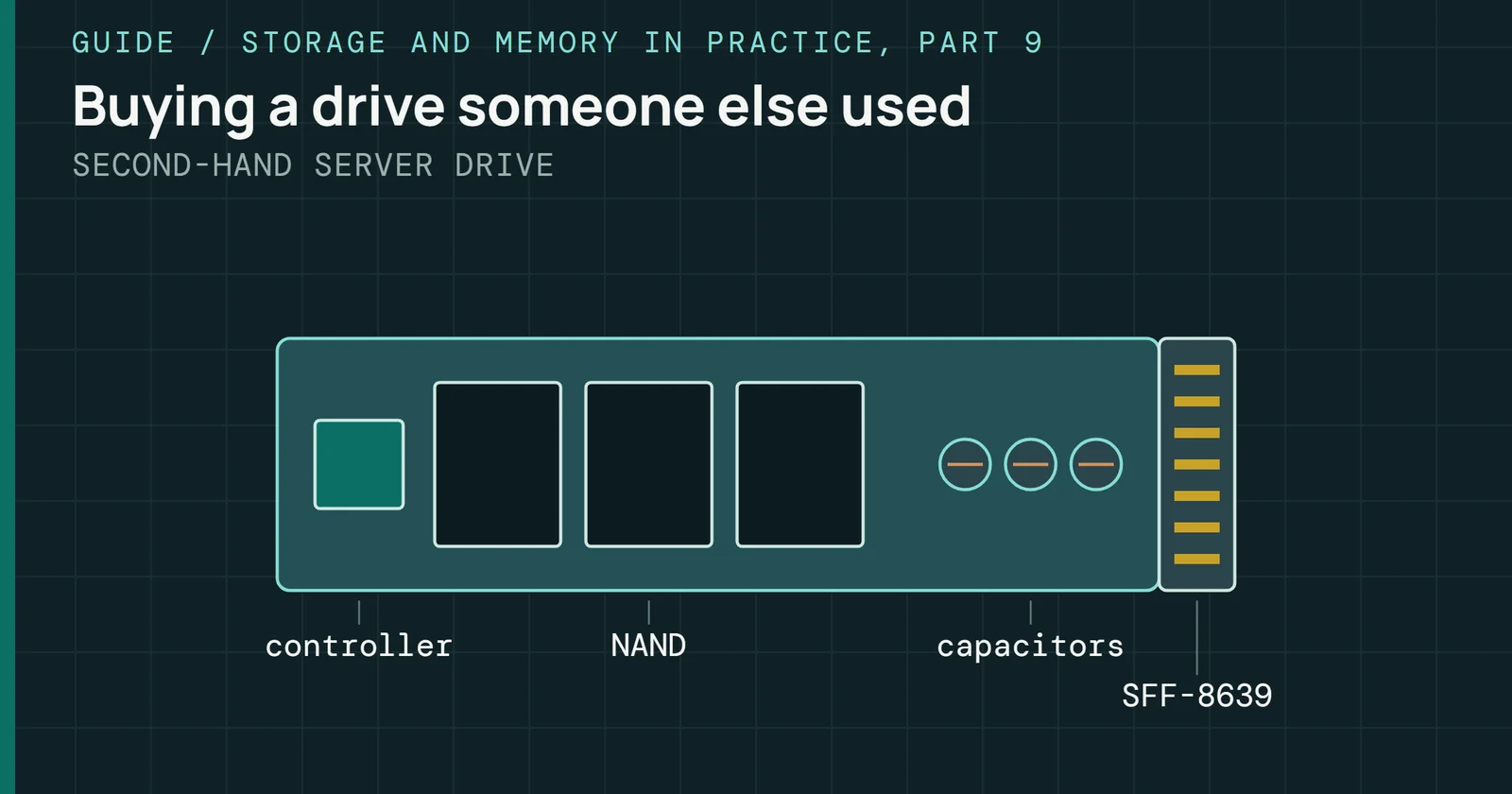
What a used data center SSD has left, how to read its SMART log, how a U.2 drive reaches a desktop, and what to check before the first write.
Memory and storage, tested and explained
NAND, SSD validation and the memory that could follow it, explained by Sean Webster through guides, sourced charts, free browser labs and open-source tools.
Atlas
One interactive 3D reference with three specimens: an NVMe SSD, an HBM stack and a DDR5 memory stick. Rotate a board or a package, click a part, and go down through it to one cell.
The SSD
Turn the driveController, NAND packages and the path between them.
HBM
Walk the stackCore dies, base die and the vertical connections through the stack.
DRAM
Read the stickA DDR5 server memory stick: its packages, the die inside and the one-transistor, one-capacitor cell that holds a bit.
Latest
Learn · November 9, 2026
What a used data center SSD has left, how to read its SMART log, how a U.2 drive reaches a desktop, and what to check before the first write.
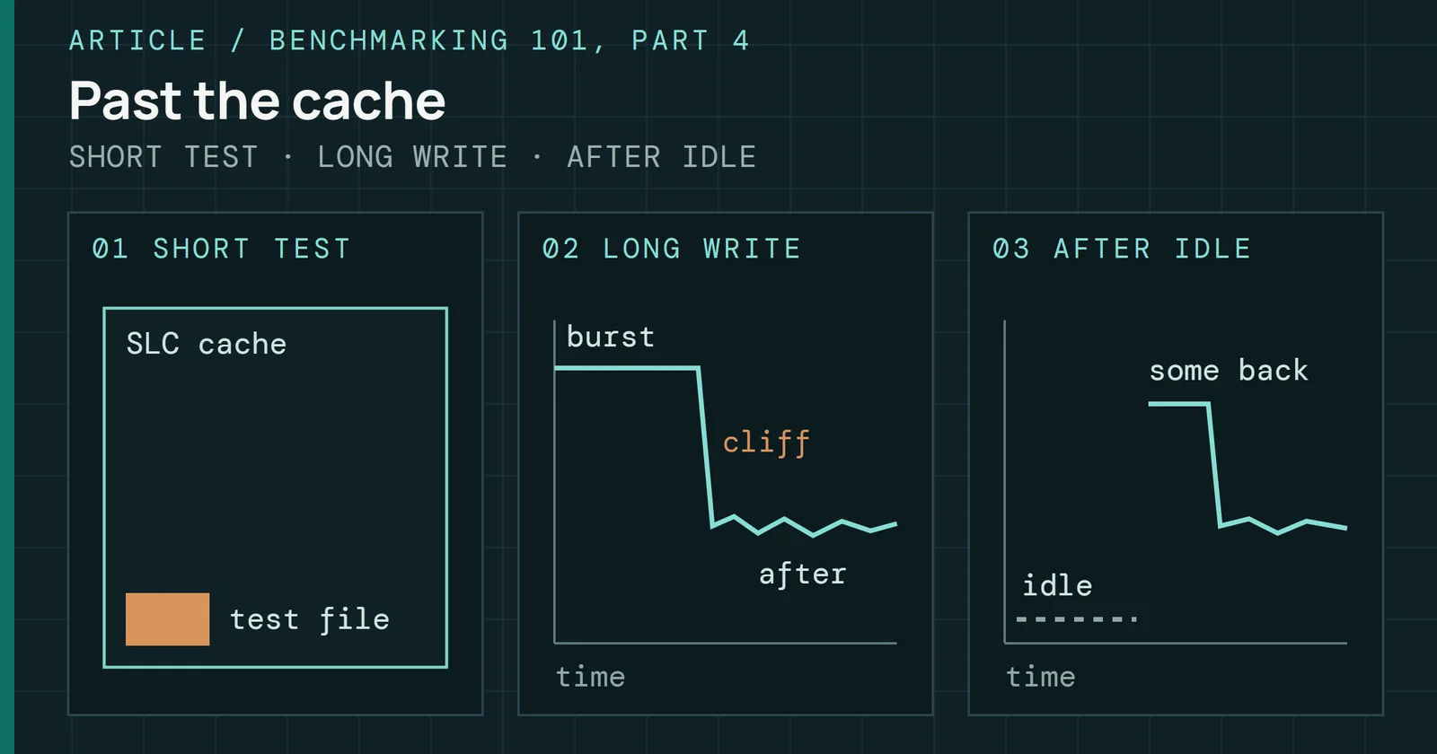
Learn · November 7, 2026
Run one long write to find where an SSD's SLC cache ends, how fast the drive writes after it, and how much speed comes back after idle.
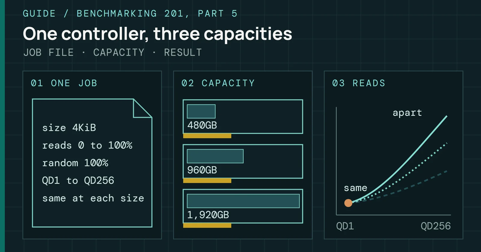
Learn · November 7, 2026
My Iometer runs on one enterprise SSD design at 480GB, 960GB and 1,920GB, and what capacity changes in random writes, deep-queue reads and sequential speed.
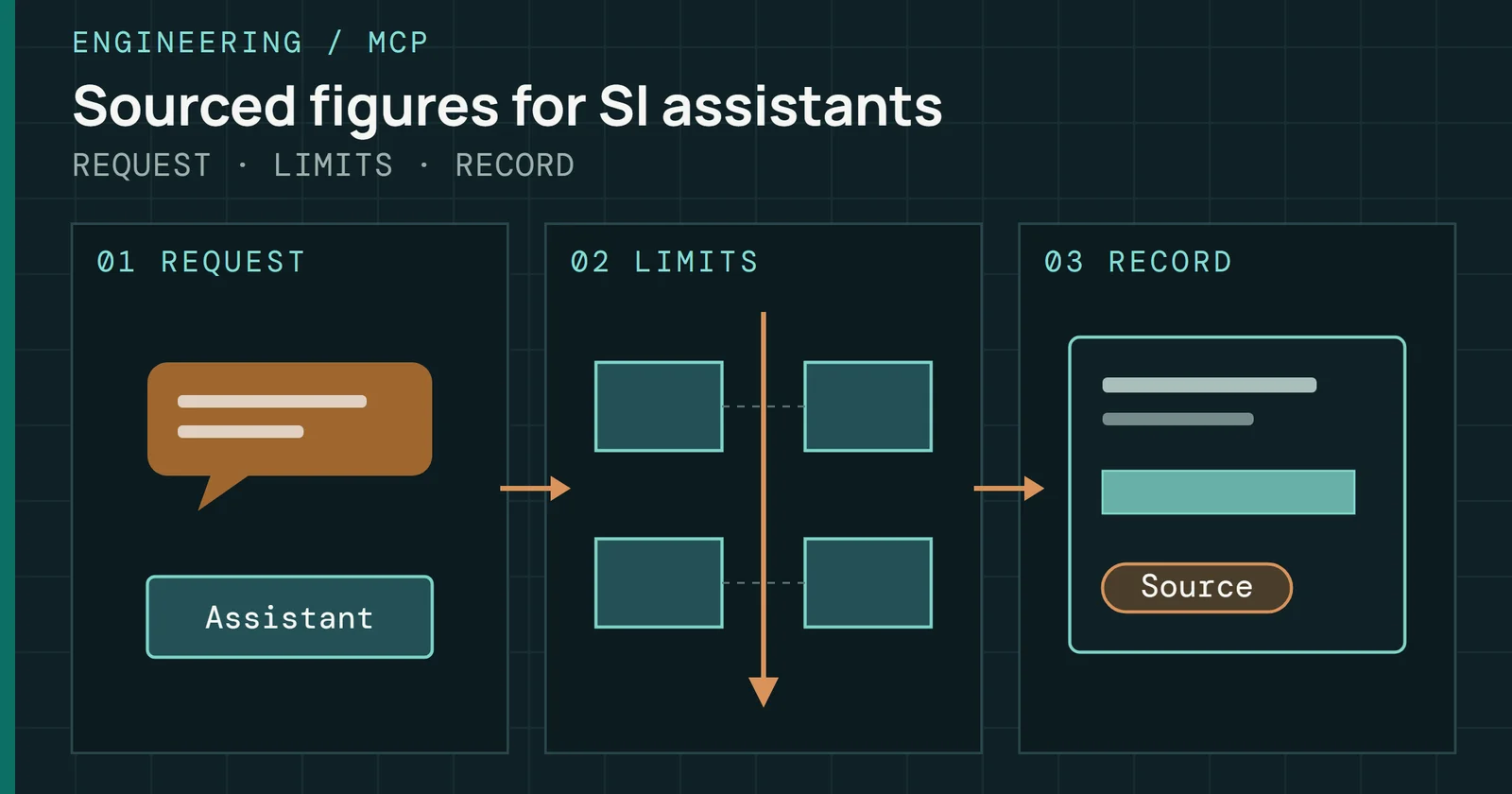
Writing · November 6, 2026
Eyes on Flash now has a public, read-only MCP server: what it serves, how to connect, which sources it leaves out, and how it runs on Cloudflare's Free plan.
Best picks
Each pick comes from a tested review and the maker's data sheet, held to a bar the page states up front. A commission never changes which products are picked or their order.
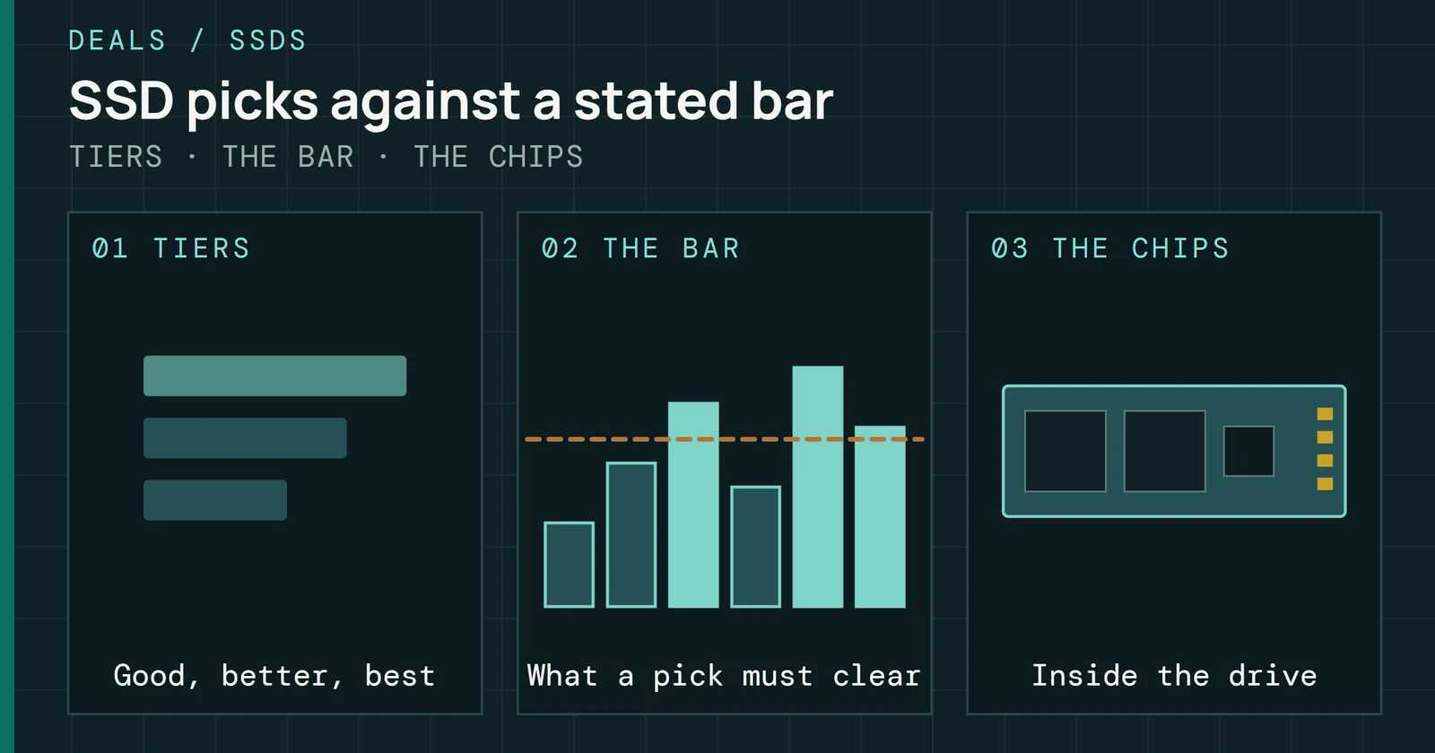
Internal and portable SSDs by tier, with the controller, DRAM and flash inside each one.
See the picks
Desktop DDR5 and DDR4 kits by tier, with the DRAM chips inside.
Internal hard drives by tier, with recording type, workload rating and warranty.
Gaming and SI graphics cards by tier, picked on memory, with chip and VRAM.
Flash drives, docks, hubs, card readers, M.2 enclosures and Switch 2 cards.
NAS boxes from two bays up, and the multi-gig switches to run them.
PS5 SSDs, Xbox Series X|S expansion cards and Steam Deck drives.
Battery backup for a NAS, a desktop, a home lab rack or an AI workstation.
Learn
Series read in order and myths checked against data. Start at Part 1 or jump to the part you need; every chart and number links to its source.
10 parts
How an SSD works, from the physics of a flash cell to the controller, the translation layer and error correction.
4 of 8 parts published
What is inside drives and the links and protections around them, starting with the memory and storage hierarchy.
6 parts
The flash soldered or slotted into phones, cards, cars and small boards, starting with UFS, the storage inside a phone.
8 of 9 parts published
Choosing, setting up and keeping drives and memory in real machines, starting with DDR5 for builders.
9 parts
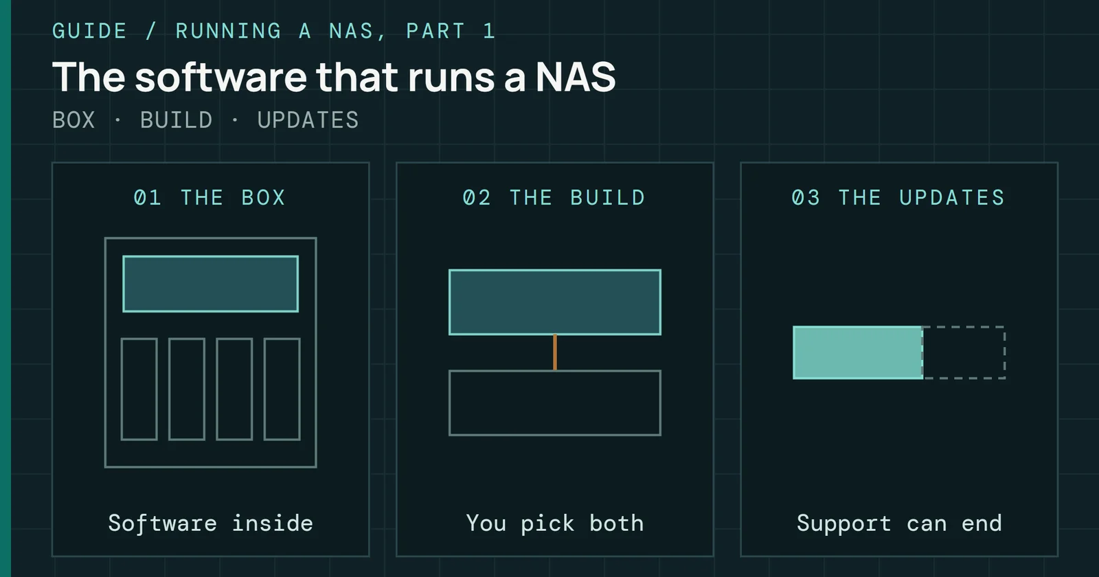
The software and setup side of a NAS, from the operating system and pools to the network, backup and the faults owners find too late.
10 parts
How to test an SSD so the number holds up: a repeatable client method in 101, then enterprise drives at steady state in 201.
7 parts
The memory a processor works from: SRAM and the cache, DRAM from the inside, what could follow DRAM, and the HBM stack.
5 parts
The non-volatile memories beside flash: NOR and on-die memory, phase-change memory and Optane, MRAM, ferroelectric and resistive memory.
6 parts
How chips are printed with light, from mercury lamps to High-NA EUV, then CoWoS and the rest of advanced packaging.
3 parts
SI itself: what a language model knows, running one on Windows, and the agents built on one.
8 parts
Memory and storage built for SI, from a memory cell used as a weight to high bandwidth flash and the drives made for inference.
5 parts
The networks that carry storage traffic for SI clusters, starting with NVMe over Fabrics.
18 myths
SSD claims, each checked against test data, the specs or a lab, with a plain verdict.
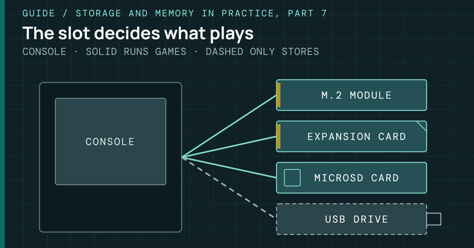
What the PS5, Xbox Series X|S, Steam Deck, other PC handhelds, and Switch 2 accept for added storage, and which of it plays games instead of only holding them.
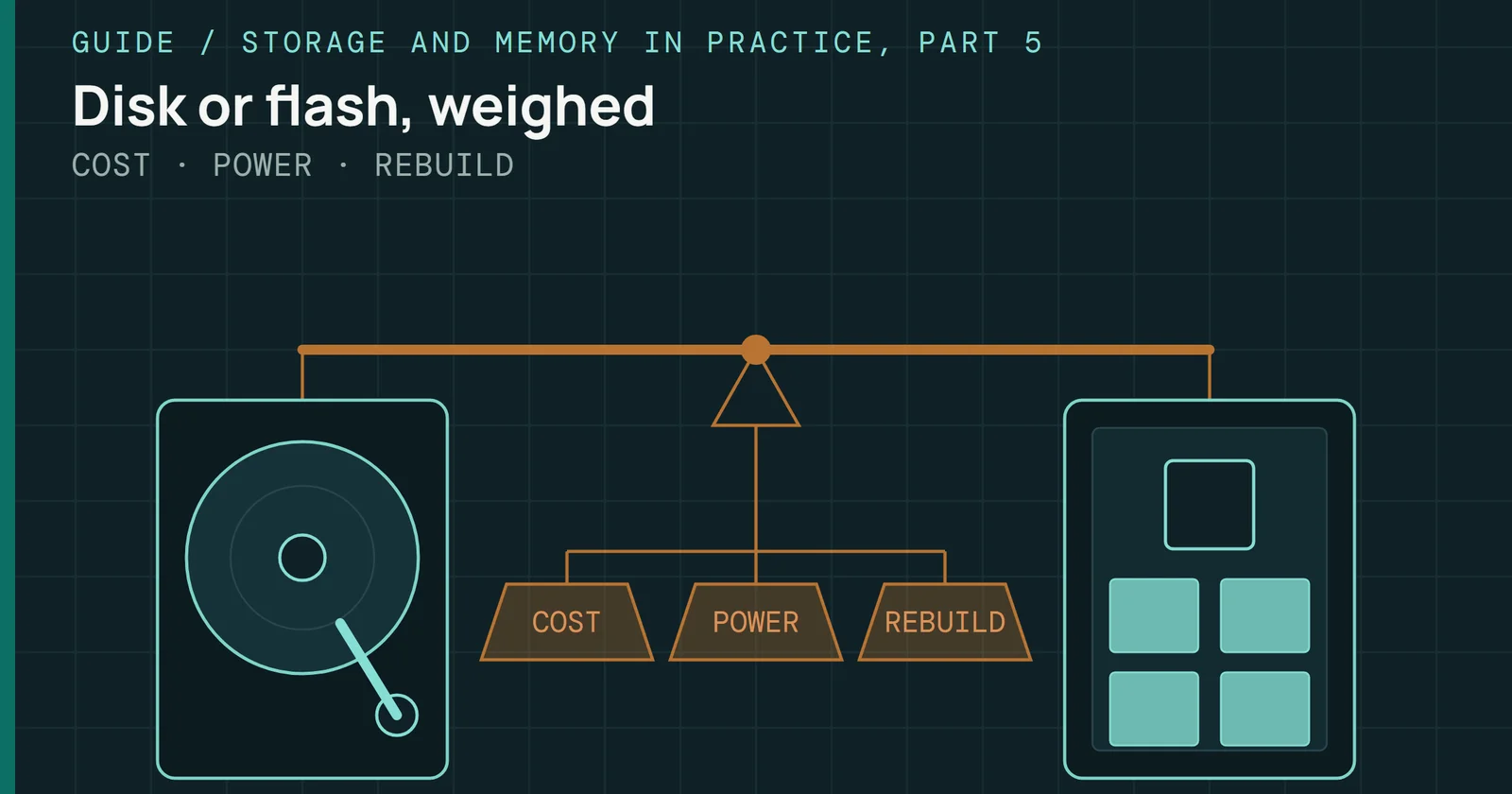
Hard drives and SSDs compared on what a terabyte costs, what each draws at idle and under load, and how long a failed drive takes to rebuild.
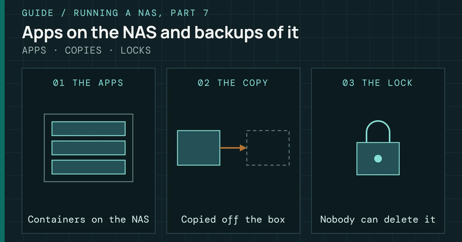
Running apps and containers on a NAS, and backing the NAS itself up with snapshots, replication, vendor tools, rclone, restic, Borg and Kopia.
Explore
Simulators and drive checks that run on your device, sourced timelines, and software to install. No uploads, no accounts.
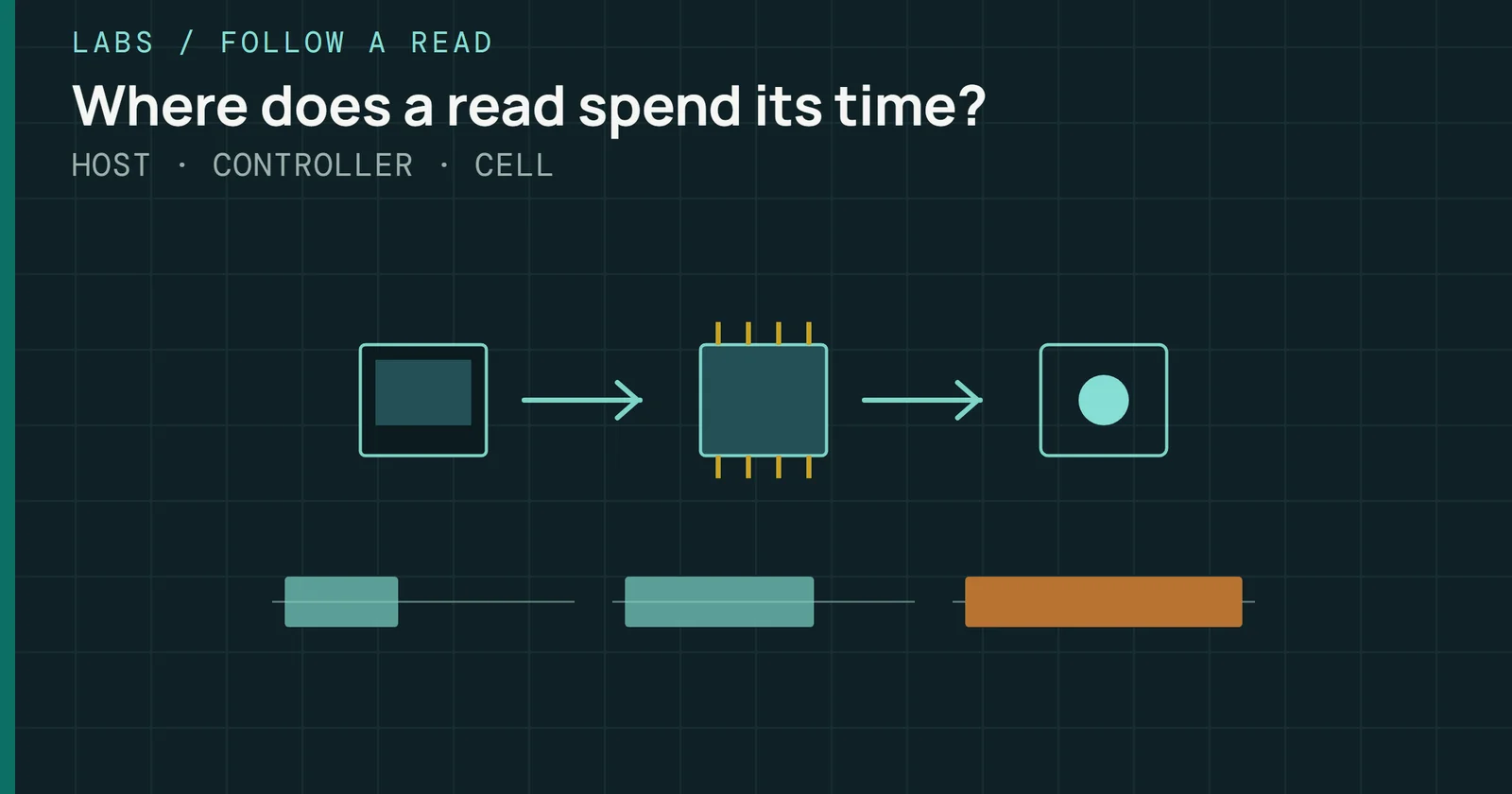
Follow one 4KiB read through a Samsung 990 Pro 2TB, from the host command to the NAND cell and back, with measured and published times for each stop.
Try this: Step through one 4KiB read in ten frames, then switch DRAM or DRAM-less and fresh or worn pages, and read the time on the bench.
Open Follow a ReadA browser tool that opens on a made-up example drive already decoded, then reads NVMe SMART / Health logs and Identify Controller data from nvme-cli, smartctl or raw hex, with endurance numbers.
Try this: Read the decoded example drive, then change the TBW rating and capacity to see remaining life.
Open NVMe SMART DecoderTry this: Switch between layers, bit density, interface speed and cell type, then click a point to see the paper behind it.
OpenTry this: Filter by host bus, sort the table, then click a point to jump to the controller brief behind it.
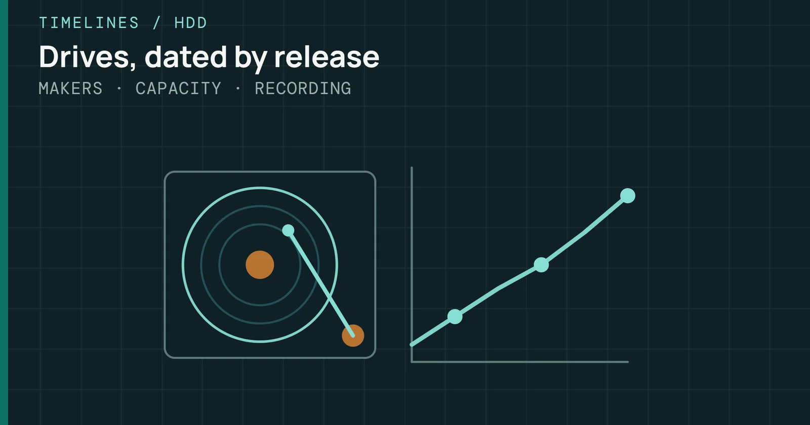
OpenTry this: Follow hard drive capacity by year, then filter by recording method to see where shingled, microwave and heat-assisted drives took over.
OpenTry this: Switch to data rate, watch the JEDEC line step up, then click a die to see the release or datasheet behind it.
OpenTry this: Compare stack bandwidth by vendor, then see which accelerators used each generation.
OpenBit Stream
43 memory, flash, controller and drive companies, every quarter: revenue, profit, forecasts and the fabs behind them, read for the drive you buy.
Bit Market · Latest quarter
Quarters are calendar quarters. Each company’s fiscal quarter goes under the calendar quarter in which it ends, except that a quarter ending in the first 7 days of a month counts as the month before. Its own label is under each figure. Won, yen, New Taiwan dollar and yuan figures are converted to US dollars at the Federal Reserve H.10 average for the quarter; the filed figure is under each. Samsung’s tile here is its chip division (Device Solutions); the tables below show the whole company.
Q3 2026 so far: 42 of 43 companies have reported. Still to report: YMTC.
News · Week ending November 13, 2026 · 15 items
Writing
Reviews, validation methods, engineering notes and reflections. My published reviews elsewhere are listed under Technical Analysis. A few notes cover Cell, the SSD guide chatbot in the corner of the page.
Newest
BlogEyes on Flash now has a public, read-only MCP server: what it serves, how to connect, which sources it leaves out, and how it runs on Cloudflare's Free plan.
Recent notes
Eyes on Flash now writes SI, not AI, after Executive Order 14434: what the order says, what it leaves alone, and how the site applies it.
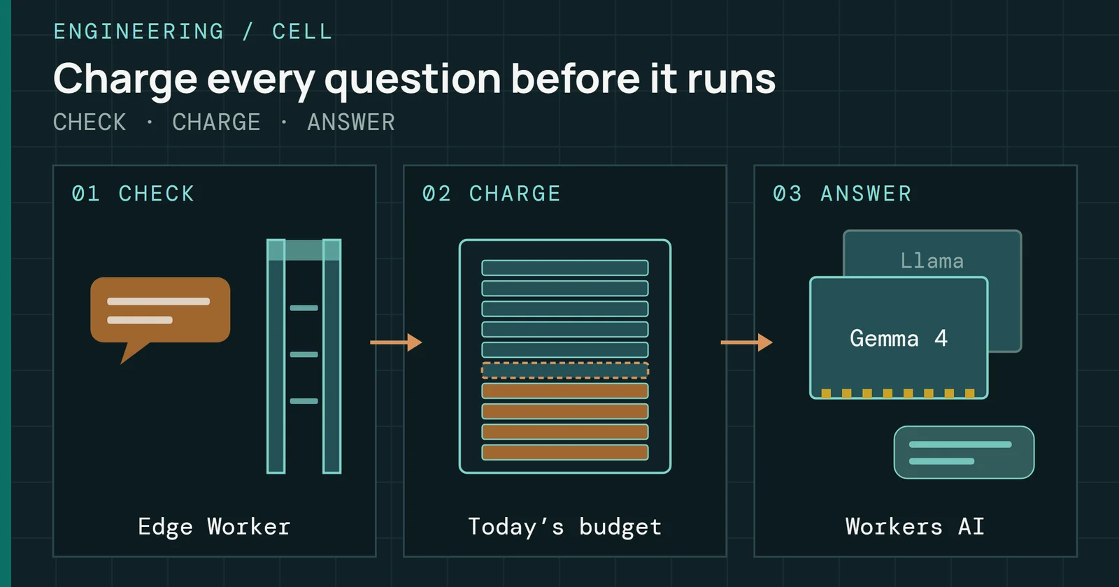
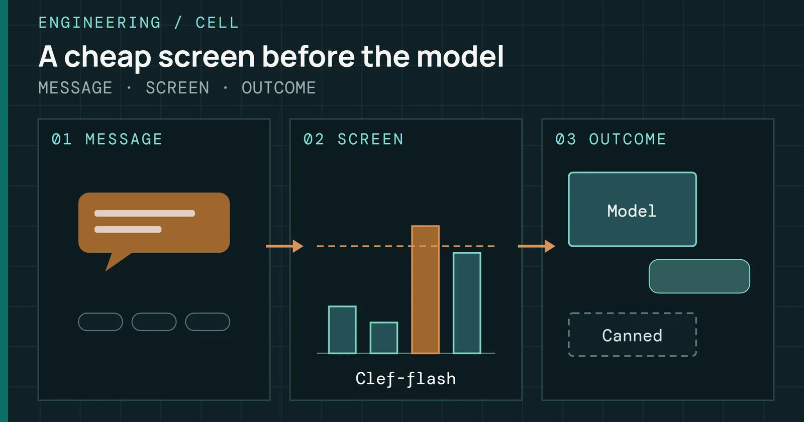
How I used Cloudflare's Clef decision model to screen off-topic and jailbreak questions for a handful of neurons before Cell's model answers.
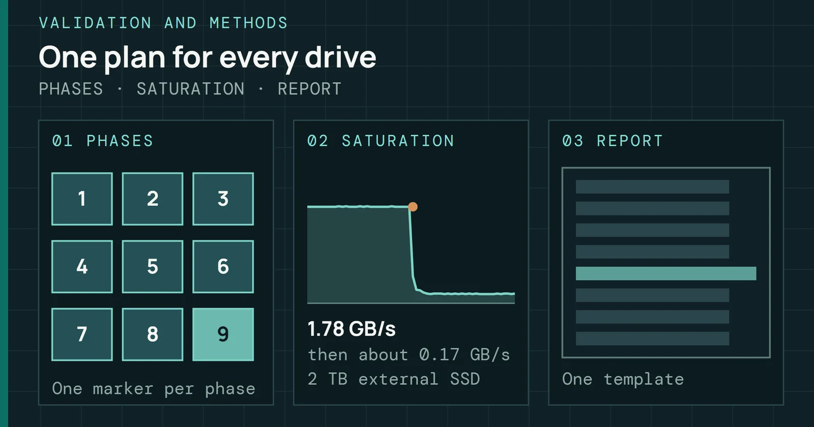
How I turned SSD validation into a repeatable process: fixed phases, write saturation with idle recovery, power capture, and a report each run had to fill in.
Research desk
Specs, standards, papers and maker news on memory and storage. Newest first. Every entry links the source.

The person behind the work
Memory and storage technologist, writer, photographer, and builder. The same instinct runs through it all: look closer, ask why, and understand how things work.