01
Connector
Links the drive to the host through PCIe and NVMe.
Take an SSD, an HBM stack and a DDR5 memory stick apart in one window, from the board down to a single memory cell.
An SSD is a coordinated collection of memory, firmware, power delivery, and high-speed signaling. Each card points to its part on the drive; open it and the Atlas takes you down through it, one named stop at a time.
Links the drive to the host through PCIe and NVMe.
Schedules I/O, manages flash, and coordinates the drive's work.
Regulates the power rails that keep the device stable.
Holds fast working data for mapping and firmware tasks.
Stores data in non-volatile flash memory packages.
Supplies local board timing; NVMe link timing still comes from the host clock.
Smooths the rails with decoupling MLCCs placed next to the loads. Some drives add a larger bank for power loss.
Stores energy each switching cycle so the regulated rails stay quiet.
Sets bias, feedback, and damping on analog and power paths.
Routes power and signals between every component.
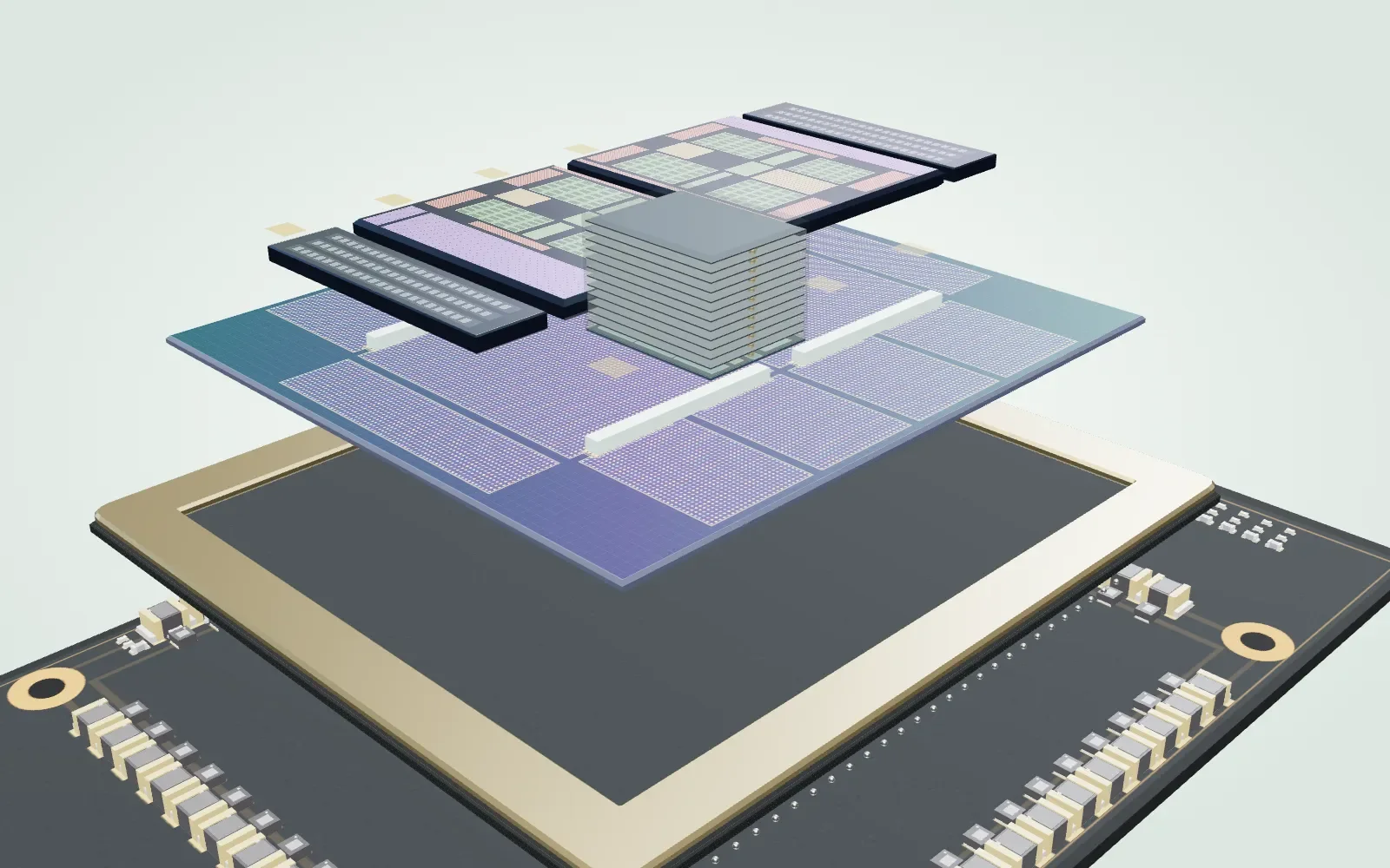
HBM is wide, stacked DRAM sitting beside compute on a 2.5D package. Here the package is pulled apart; each layer card points to where that layer sits, top to bottom.
One of the 12 DRAM dies, with bank arrays on both sides of a central stripe of vias and control strips between them.
Open in the AtlasOne HBM stack on its own: a base die under a 12-high pile of DRAM core dies. Twelve is the height drawn, a representative option rather than a measured count.
Open in the AtlasThe logic die at the bottom of the stack. Its face shows the interface (PHY) band, the through-silicon via area and a test port, as published floorplans describe.
Open in the AtlasA reference accelerator layout: compute dies, eight HBM stacks, an LSI bridge, and the substrate beneath them.
Open in the AtlasVertical copper connections that carry signals and power through each die.
Open in the AtlasKeep going from the die down to a bank and the one-transistor, one-capacitor cell that stores a single bit.
Open in the AtlasThe same read in DRAM: controller, PHY, channel, then the commands that open a row, read it and close it again at the cell.
Open in the AtlasThe DRAM specimen is a DDR5 server memory stick, an RDIMM with ECC. Its packages share the board with the parts that buffer, power and identify it; open one package and the Atlas goes down through the die to a single cell.
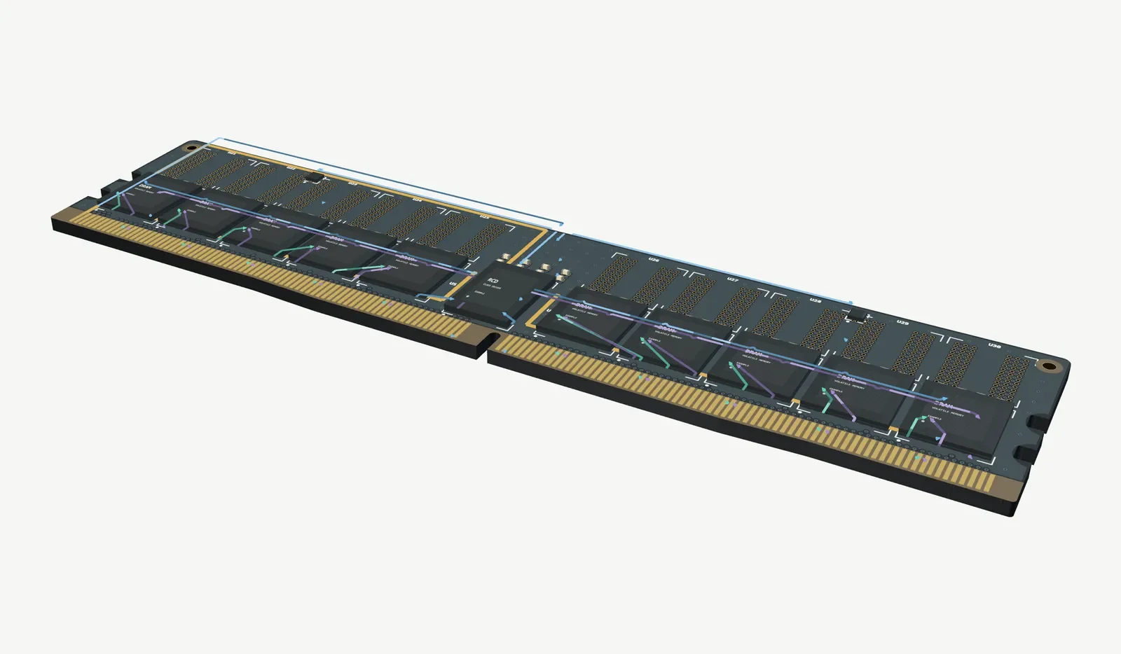
Buffers the command, address and clock lines, so the memory controller drives one load instead of every package.
Open in the AtlasDDR5 moved regulation onto the stick: the PMIC turns the board supply into the core, I/O and pump rails.
Open in the AtlasHolds the stick’s identity and timings for the system to read at start, and reaches the temperature sensors.
Open in the AtlasPins front and back carry two independent subchannels, clock, command and power. The key notch fits a DDR5 slot only.
Open in the AtlasThe die lies face down on a substrate under the mold, wired through a slot to the solder balls.
Open in the AtlasBanks gathered into bank groups around a central stripe of control logic and pads.
Open in the AtlasOpens one row at a time: ACTIVATE opens it, READ follows, PRECHARGE closes it again.
Open in the AtlasRows of mats, each a field of cells with row drivers on one side and sense amplifiers on the other.
Open in the AtlasThe row buffer: when a row opens they read every cell on it at once.
Open in the AtlasOne transistor and one capacitor. The charge leaks, so every cell is refreshed again and again.
Open in the AtlasEach row is one depth in the Atlas, with the SSD, HBM and the DDR5 stick side by side, so you can watch a NAND die and two DRAM dies shrink to one cell together. Every render opens at that exact stop.
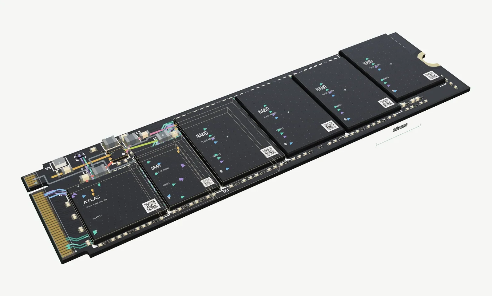
SSDReference NVMe SSD
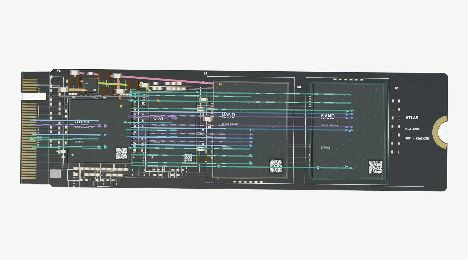
A generic M.2 2280 drive: controller, DRAM and NAND packages on both faces, and the parts that power them.
Open here in the Atlas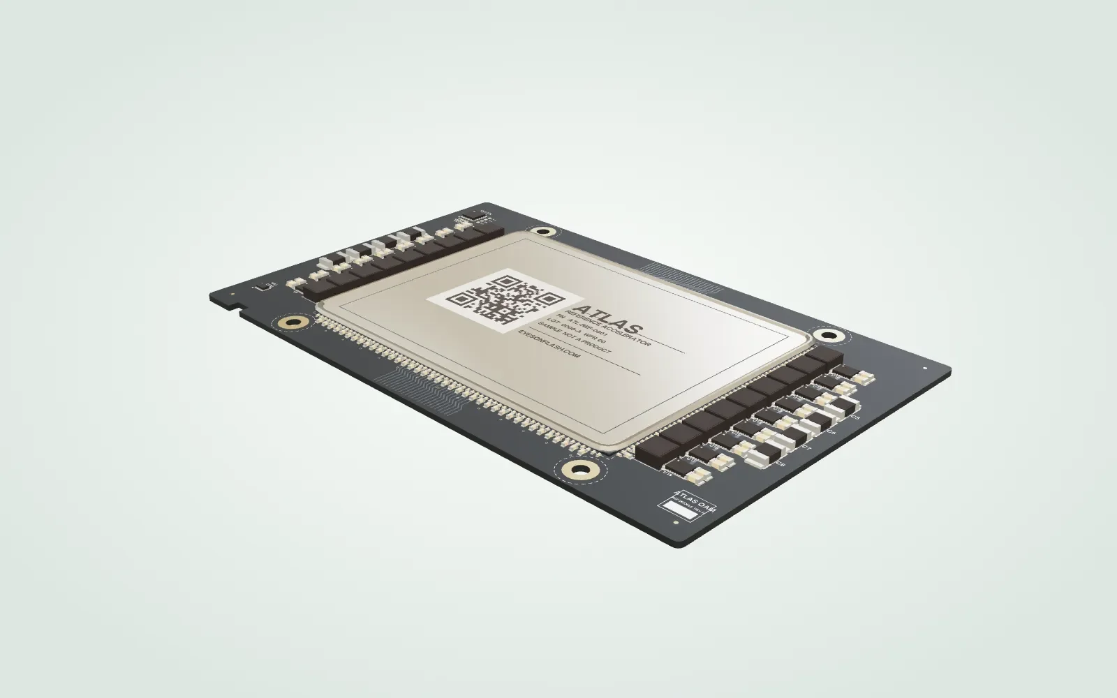
HBMPackage
A reference SI accelerator package, lid on: compute and HBM stacks sit underneath.
Open here in the AtlasDRAMDDR5 RDIMM
A DDR5 server memory stick with ECC: DRAM packages, the registering clock driver, its power and the edge pins.
133.35 × 31.25 mm sticksource
Open here in the Atlas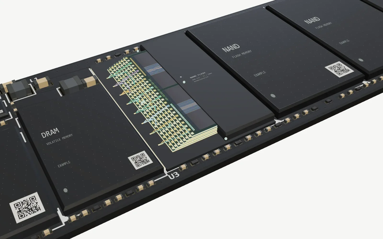
SSDNAND package
One NAND package, opened up on the board.
14 × 18 mm bodysource
Open here in the Atlas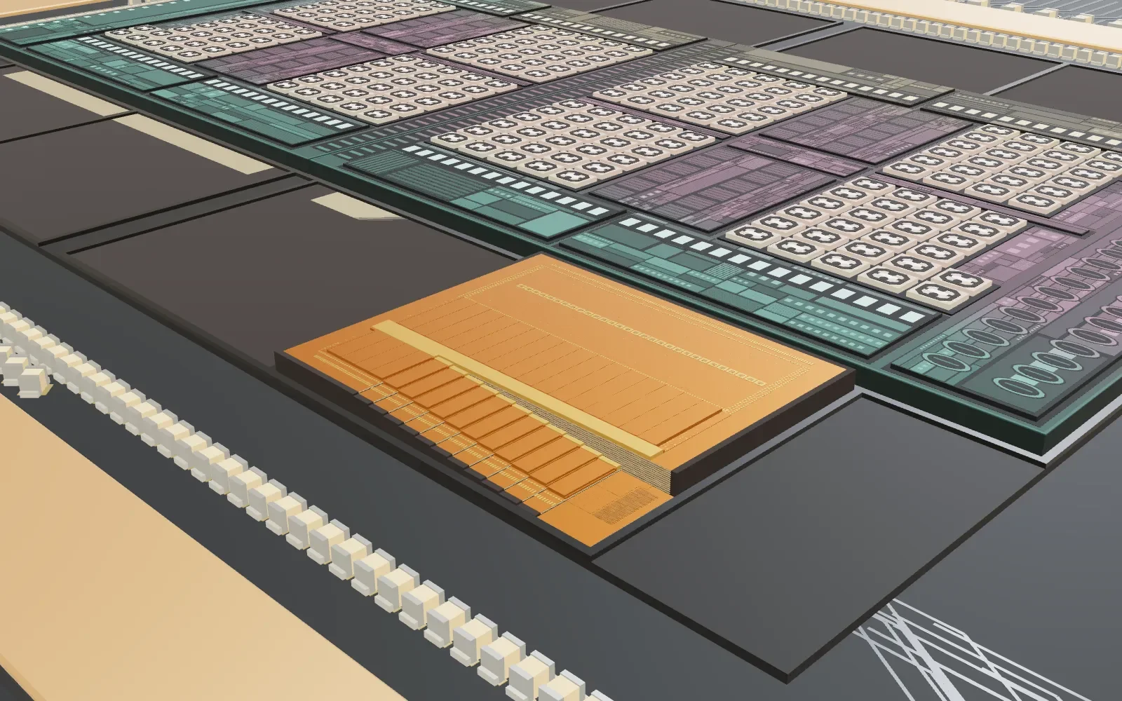
HBMHBM stack
Lid off: an HBM stack beside the compute dies.
14.175 × 10.975 mm HBM4 bodysource
Open here in the Atlas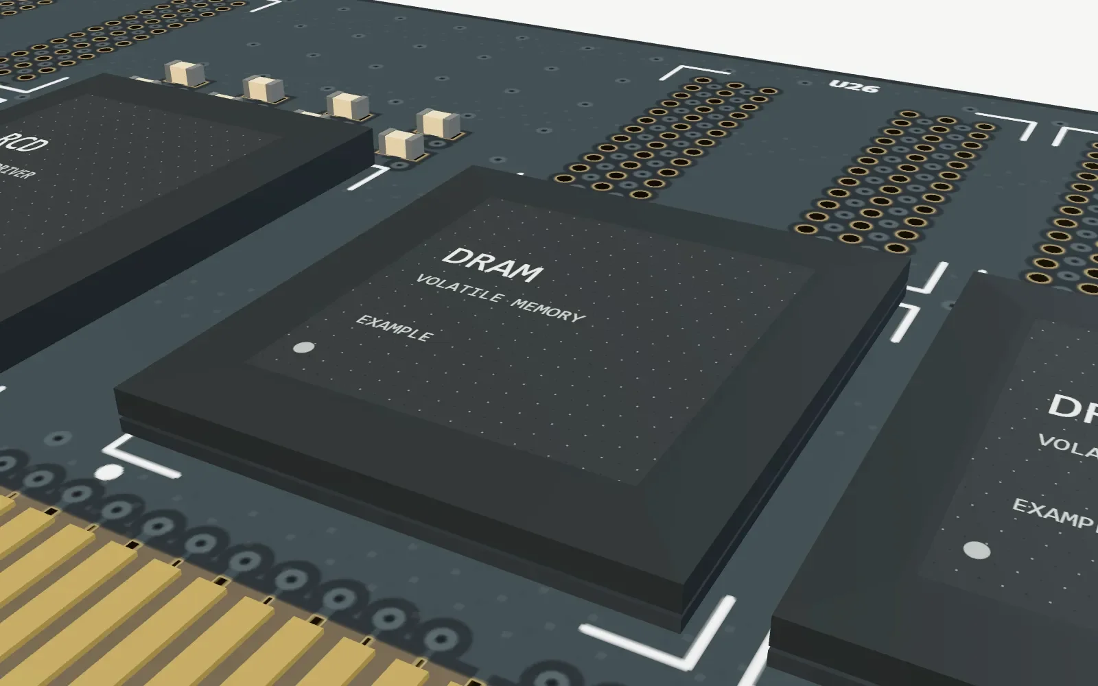
DRAMDRAM package
One DRAM package on the stick: the die sits inside, face down on its substrate.
10.0 × 11.0 mm bodysource
Open here in the Atlas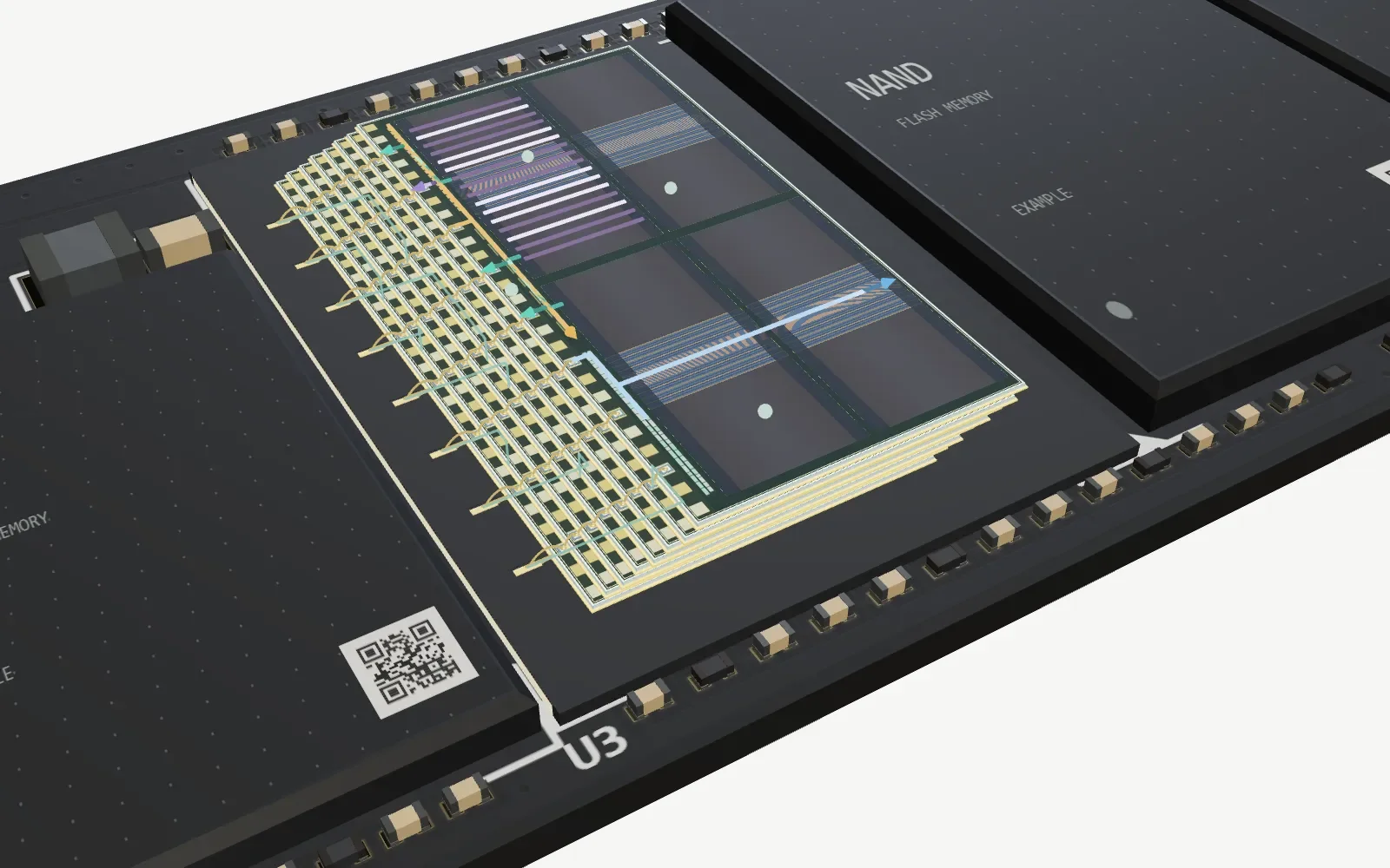
SSDNAND die
The die inside, with its planes and the periphery that drives them.
128.5 mm² for a 64-layer diesource
Open here in the Atlas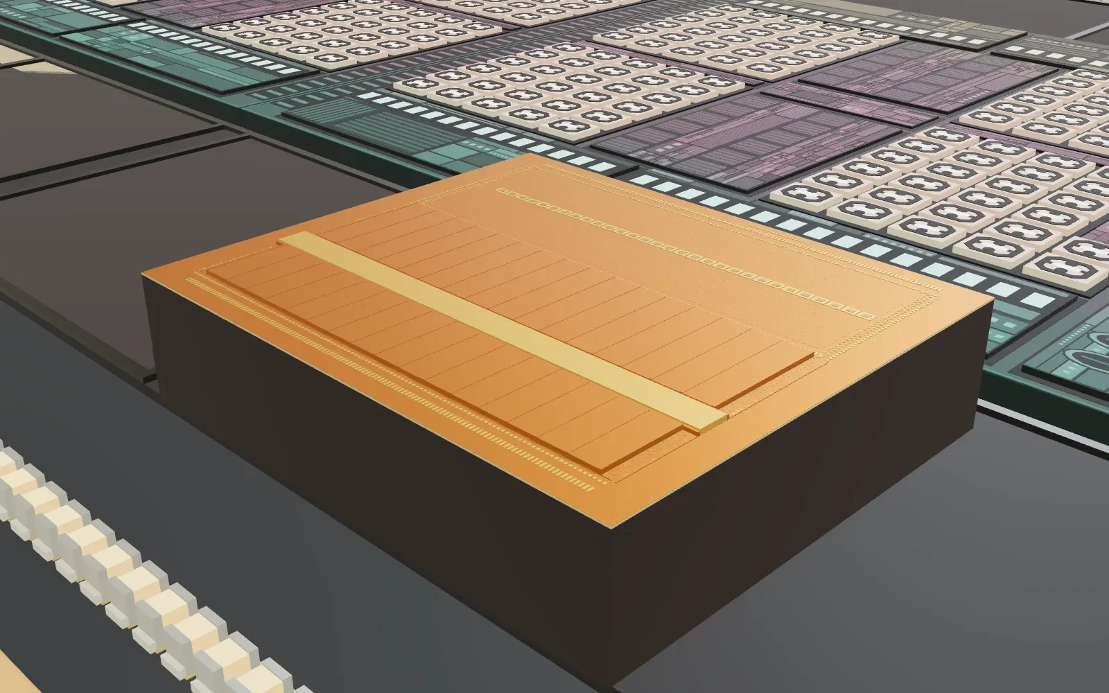
HBMCore DRAM die
One core DRAM die in the stack, above the base die.
12.8 × 11 mm Samsung HBM4 diesource
Open here in the Atlas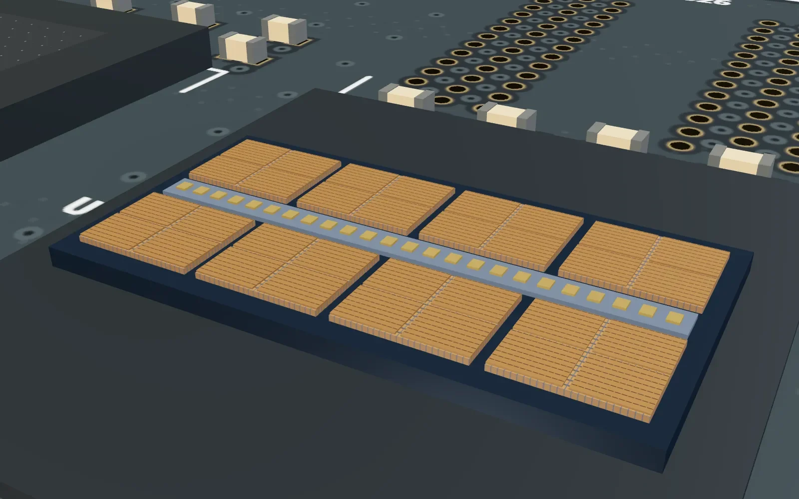
DRAMDRAM die
The die, drawn face up: its banks sit either side of a central stripe of control logic and pads.
66.26 mm² for a Micron 16 Gb DDR5 diesource
Open here in the Atlas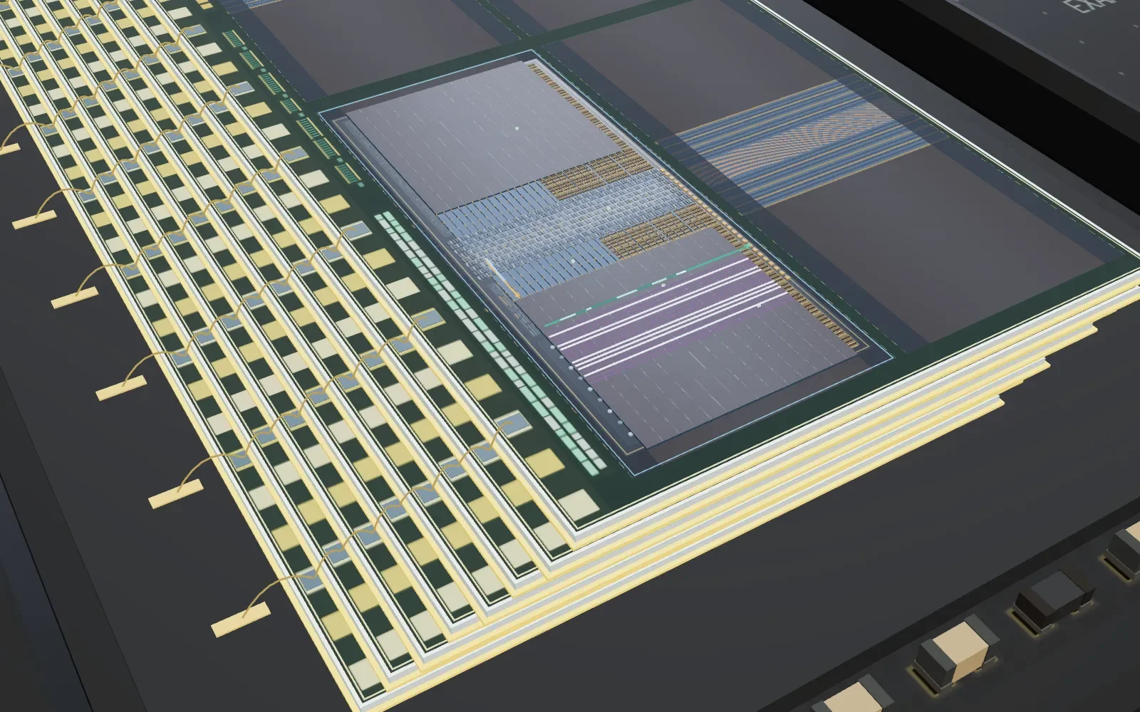
SSDMemory plane
A memory plane: blocks of vertical strings, read a page at a time.
9.4 µm tall stringssource
Open here in the Atlas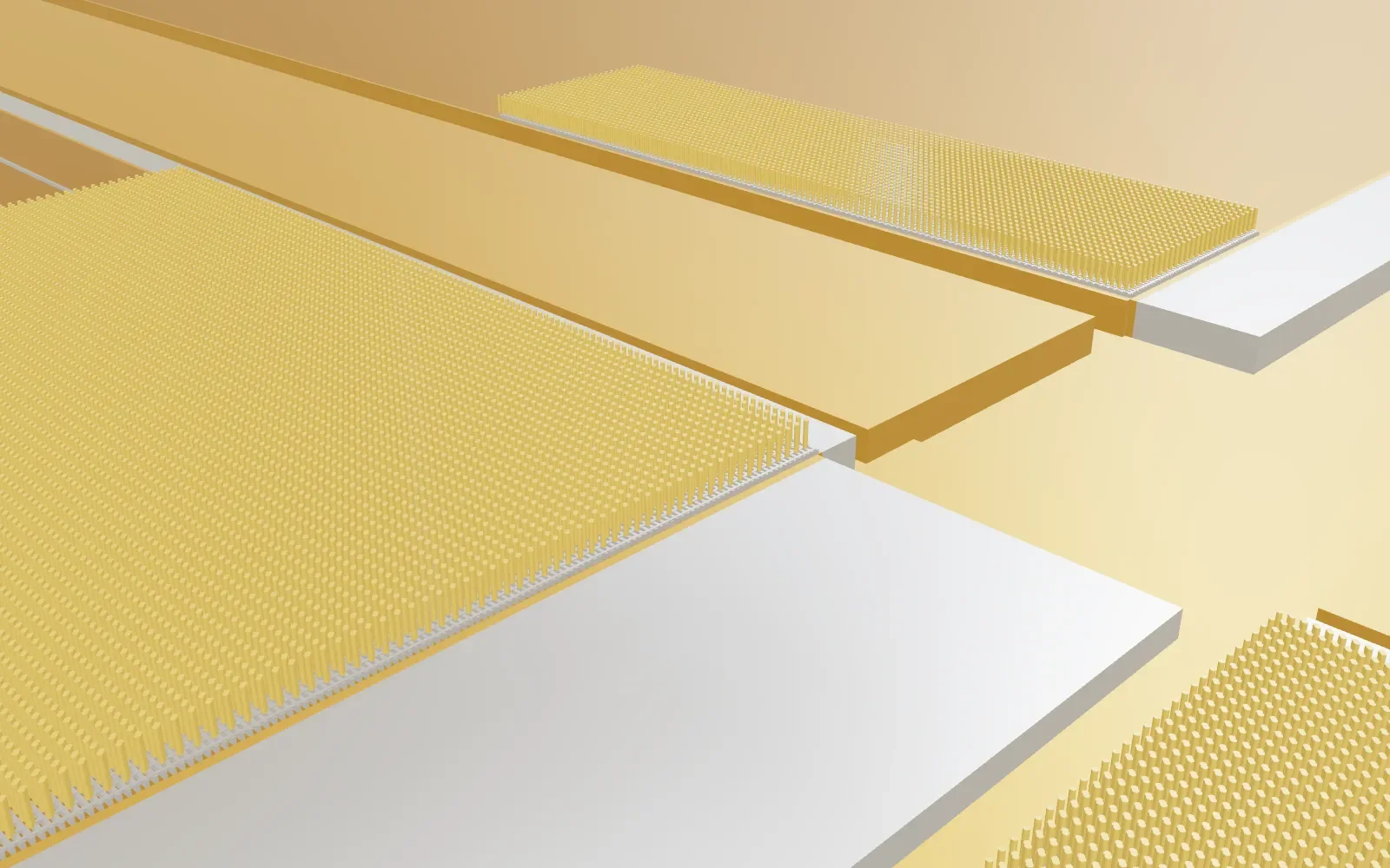
HBMCell array
A 16 by 16 patch of cells, capacitors standing over their transistors.
0.80 × 0.53 µm patchsource
Open here in the Atlas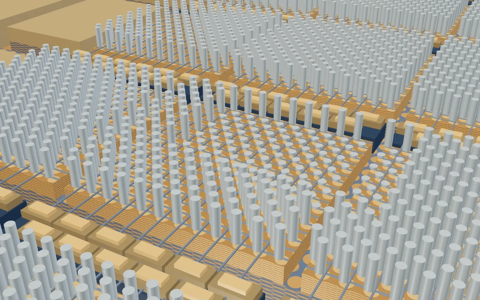
DRAMSubarray
A bank built from rows of mats, row drivers on one side and sense amplifiers on the other.
Half a million to a million cells per matsource
Open here in the Atlas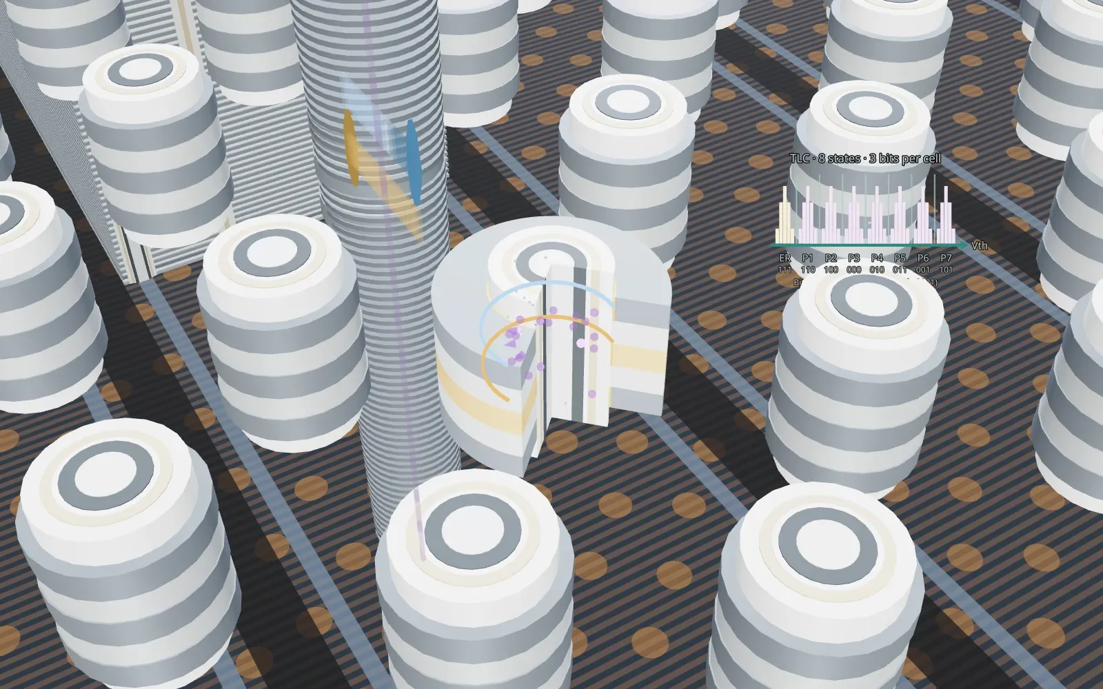
SSDCharge-trap cell
One charge-trap cell, cut open around its channel.
152 nm hole pitchsource
Open here in the Atlas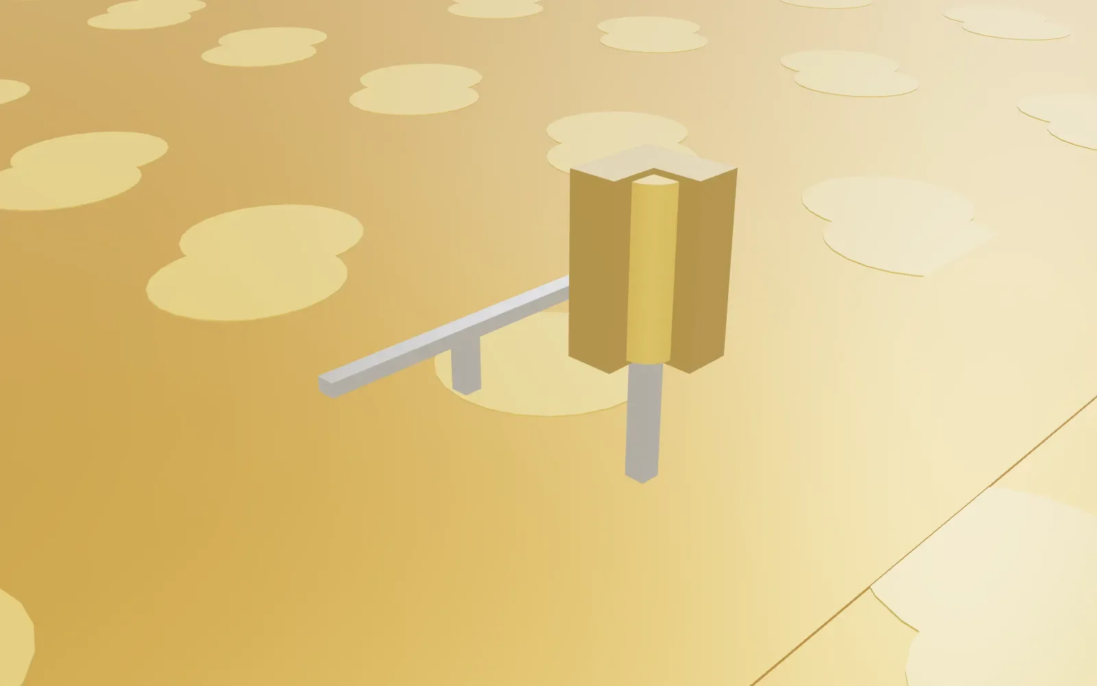
HBM1T1C cell
One bit: a capacitor and the transistor that opens it.
1,672 nm² cellsource
Open here in the Atlas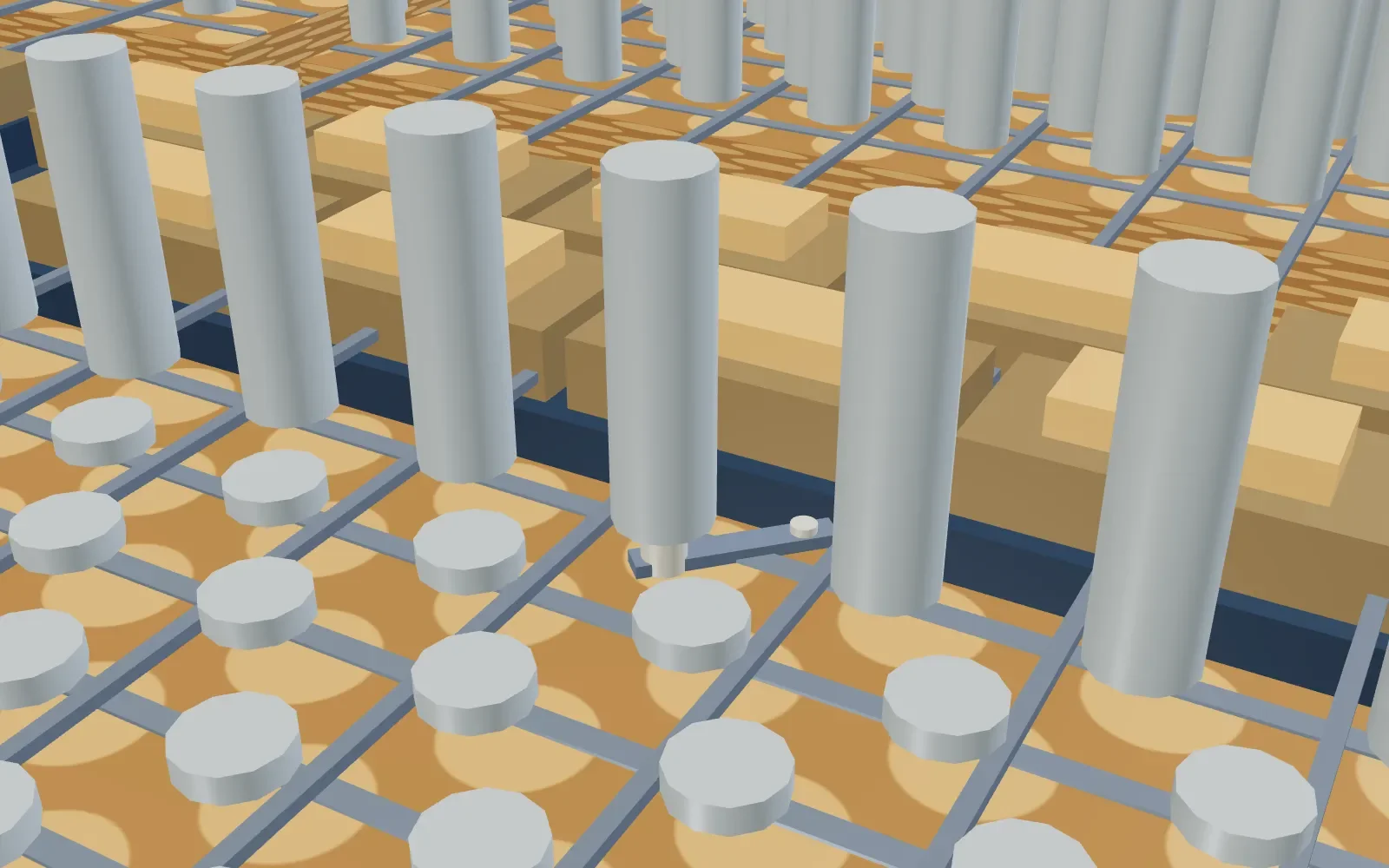
DRAMDRAM cell
One transistor and one capacitor, rewritten again and again before its charge leaks away.
Open here in the AtlasThe same read, traced three times: from the controller to a NAND cell, from the memory controller through the PHY to an HBM row that opens, reads and closes, and from the memory controller down a DDR5 stick to a bank and back out on the pins.
The Atlas shows where everything sits. These simulators run in your browser and open up the parts that carry most of the behavior: the flash cell, the firmware that manages it, and the capacitors that decide what survives a power cut. They are teaching models, not vendor data.
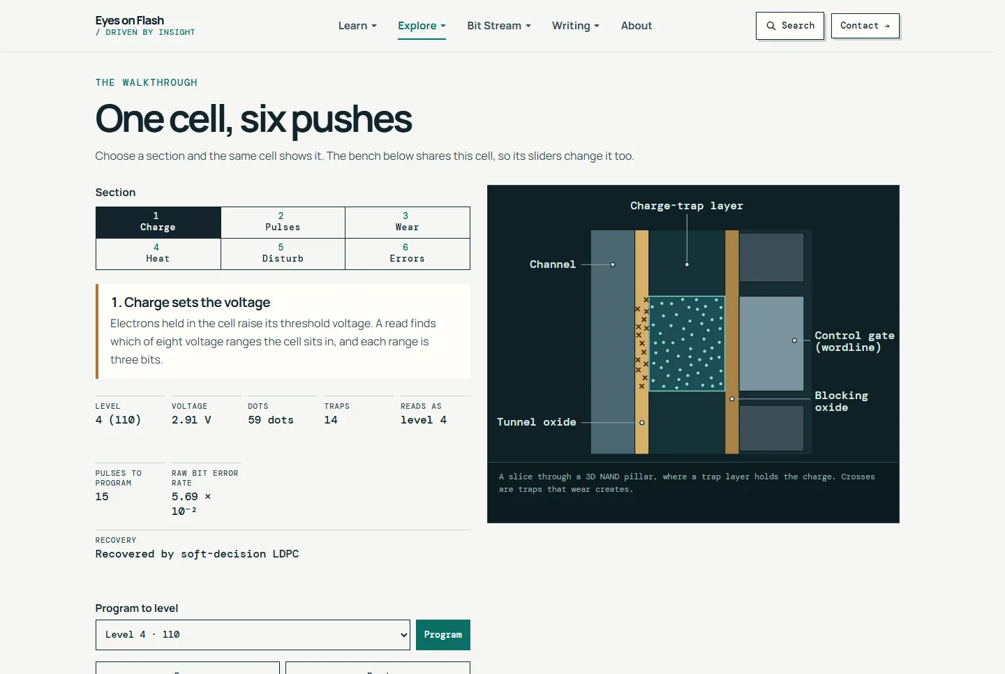
An interactive threshold-voltage simulator that shows how P/E cycling, retention, temperature and read disturb push NAND cells toward bit errors.
Try this: Choose Wear in the walkthrough, then drag a read reference on the bench chart and watch the error-correction ladder change.
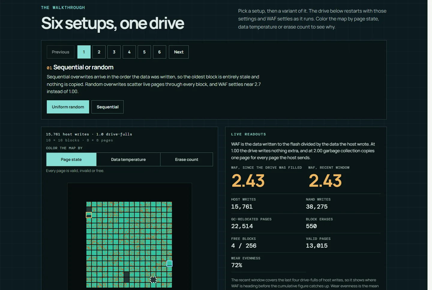
Open NAND Cell LabA flash translation layer and garbage-collection simulator that shows how overprovisioning, workload, TRIM and data placement change write amplification.
Try this: The card opens the 80-20 hot-cold drive from setup 4, Hot and cold data. Choose Separated and give it about 30 seconds: write amplification settles near 2.2 instead of about 2.4.
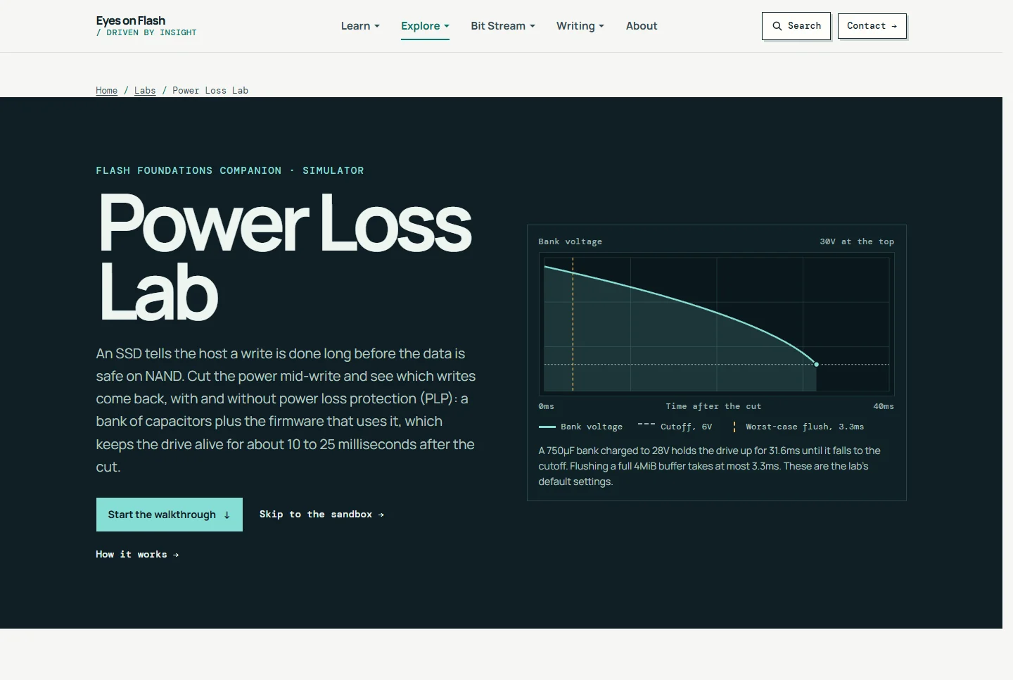
Open FTL & GC SandboxCut power to a simulated SSD mid-write and see which writes come back, with and without capacitor-backed power loss protection, old capacitors and flushes.
Try this: Scroll the five sections to see what capacitors, fsync and age change, then drag any setting in the sandbox and watch the cells.
Open Power Loss LabOrbit the model, pick a part, and swap between the SSD, HBM and DRAM without losing your place in any of them.