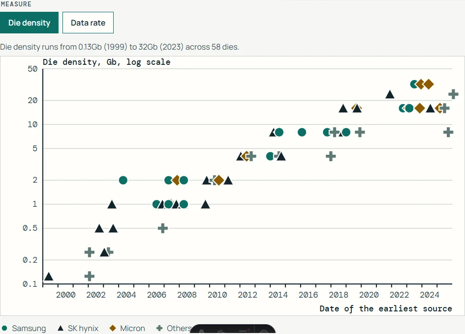
DRAM is sold under four families, and each one is built for a different job. DDR5 is built for client systems and high-performance servers. LPDDR is low power memory, and JEDEC names 5G and AI applications for it. GDDR is graphics memory. HBM stacks DRAM dies, and HBM4 has a 2,048-bit interface. All four families share a one-transistor, one-capacitor cell, but the interface, the package and the speed differ.
Working Memory
Working Memory, Part 5: Current Memory ICs
A sourced guide to the DRAM chips in use now: DDR5, LPDDR5X, GDDR7 and HBM3E and HBM4, what is shipping, what is only sampling, and what is still research.
On this page 13 sections
This part of Working Memory is a map of the DRAM that exists now, with the source for each number next to it, and it leaves NAND out. I only count a part as shipping when a maker or a customer says it is. A part that is sampling has gone to customers for testing, and a part that is announced may still be months from a shelf. Where I have no maker or JEDEC page for something, I say so instead of filling the gap. Working Memory, Part 2 explains the DRAM cell and the DDR bus, Working Memory, Part 4 covers stacked DRAM, and the dates behind each family are on the DRAM die timeline and the HBM timeline.
How to read the numbers
Three habits keep the tables honest:
- Shipping, sampling or developed: a press release that says a company has developed a part is not a product. I label each part with the wording its maker used.
- Gb or GB: a lowercase b is a bit and an uppercase B is a byte. A 16Gb die holds 2GB. Die density is quoted in gigabits and module or stack capacity in gigabytes.
- MT/s or Gb/s: MT/s is transfers per second on one pin, and Gb/s per pin is the same number written in bits. DDR5-6400 means 6,400MT/s, or 6.4Gb/s on each data pin. Total bandwidth is that rate times the number of pins, divided by eight.
How to read the numbers
A 16Gb die is 2GB, and 6,400MT/s is 6.4Gb/s
Three habits. The middle and right panels use this section's own examples.
A 16Gb die in the middle panel holds 2GB, and the right panel is the DDR5-6400 example, 6,400MT/s and 6.4Gb/s.
Every maker figure is the maker’s own claim against a baseline the maker chose, and I mark it as vendor data.
DDR5
DDR5 is JEDEC’s standard for client systems and high-performance servers. JEDEC published it on July 14, 2020. It doubled the burst length to 16, doubled the banks from 16 to 32 on dies of 16Gb and above in x4 and x8 parts, gave each module two independent 40-bit sub-channels, and cut the supply voltage from 1.2V to 1.1V. It launched at 4.8Gb/s per pin.
DDR5
Maker pages list faster DDR5 pin rates than launch
Bar length is Gb/s. Each label keeps the unit the source printed.
Bar length is in Gb/s, so the 6,800Mb/s bar ends between the 5 and 7.5 ticks, and the label keeps the unit its source printed.
DDR5 kept moving after launch. In April 2024, JESD79-5C extended the timing definitions from 6,800Mb/s to 8,800Mb/s. On JEDEC’s page the current edition is JESD79-5D, version 1.41, from November 2025, and that page doesn’t print a speed, so I don’t quote one for it.
Makers list faster parts than the standard text. Micron’s DDR5 page lists registered modules (RDIMMs) up to 9,200MT/s and multiplexed-rank modules (MRDIMMs) up to 8,800MT/s, with 128GB RDIMMs built from 32Gb monolithic dies.
On density, Samsung announced a 12nm-class 32Gb DDR5 die in September 2023. SK hynix reported that a 256GB server RDIMM completed Intel Data Center Certification in December 2025. That compatibility validation was on Xeon 6. The module is built from 32Gb dies on its fifth-generation 10nm-class (1b) process. A certification is not a sales announcement, so I do not count it as shipping.
LPDDR5, LPDDR5X, LPDDR5T and LPDDR6
LPDDR is JEDEC’s low-power DRAM family. JEDEC published JESD209-5 in February 2019 as the LPDDR5 standard and targeted 6,400MT/s. The JESD209-5B revision of July 2021 extended it to 8,533Mb/s and added LPDDR5X as an optional extension.
LPDDR5, LPDDR5X, LPDDR5T and LPDDR6
LPDDR pin rates cluster near 10.7Gb/s
Bar length is Gb/s. Each label keeps the unit the source printed.
Neutral bars are the JEDEC rates, 6,400MT/s and 8,533Mb/s, and copper bars are the maker rates, 9.6Gbps and 10.7Gbps.
Makers have gone faster still. SK hynix announced LPDDR5T (the T stands for Turbo) in January 2023: 9.6Gbps, 13% faster than LPDDR5X by its count, with samples sent to customers. Micron shipped qualification samples of the first LPDDR5X on its 1γ (1-gamma) node at 10.7Gbps in June 2025. Qualification samples mean testing, so this is sampling and short of volume. For die size, TechInsights measured Samsung’s D1b 16Gb LPDDR5X at 36.68mm². A teardown firm made that measurement and the maker made no claim about it, so it is a secondary source.
JEDEC published LPDDR6 as JESD209-6 on July 9, 2025. A die has two sub-channels, each with 12 data lines.
Two makers have LPDDR6 parts, and neither says volume production yet. SK hynix said on March 10, 2026 that it had developed a 16Gb LPDDR6 die on its 1c process, which is the sixth generation of its 10nm class, with a base speed over 10.7Gbps, and that it plans to begin supply in the second half of 2026. Samsung said in September 2026 that its 16GB LPDDR6 was validated at up to 10.7Gbps on a Qualcomm Snapdragon platform, with up to 114GB/s of bandwidth and up to 21% better power efficiency than LPDDR5X. Samsung also says it has completed sampling. Sampling and validation on a customer’s platform come before shipping, so I list both as not shipping yet. I have no Micron page for an LPDDR6 part.
The newest use of LPDDR is a server module on a small board called SOCAMM2. SK hynix said on April 20, 2026 that it began mass production of a 192GB SOCAMM2 on its 1cnm LPDDR5X. That is the sixth generation of its 10-nanometer-class process. Micron sampled a 256GB SOCAMM2 in March 2026. The module is covered in the CAMM2 guide.
GDDR6X and GDDR7
GDDR is graphics memory, and JEDEC’s GDDR7 release names graphics, gaming and AI. JEDEC published GDDR7 as JESD239 on March 5, 2024. It is the first JEDEC DRAM to use PAM signaling, a three-level (PAM3) interface that sends three bits over two cycles. It doubles the independent channels from two to four and reaches up to 192GB/s per device.
GDDR6X and GDDR7
GDDR7 pin rates sit above GDDR6X
Each bar is the high rate that source prints, in Gb/s per pin.
Copper marks a memory part, and the neutral bar is the RTX 5090 at 28Gb/s.
Samsung announced the first GDDR7 in July 2023 as a 16Gbit part at 32Gb/s per pin, and SK hynix said in July 2024 that its GDDR7 runs at 32Gbps per pin and can reach 40Gbps depending on conditions. In a product, NVIDIA’s RTX Blackwell whitepaper lists the GeForce RTX 5090 with 28Gb/s GDDR7 on a 512-bit interface, 1.792TB/s of peak bandwidth. That 28Gb/s sits below the 32Gb/s the first dies were announced at.
GDDR6X is Micron’s own PAM4 graphics memory, and JEDEC calls GDDR7 the first JEDEC standard DRAM to use PAM signaling. GDDR6X launched in September 2020 as an 8Gb die at 19 to 21Gb/s. In April 2022 Micron put a 16Gb GDDR6X into volume production for the GeForce RTX 3090 Ti, running at 21Gb/s there, with a roadmap to 24Gb/s. Micron’s current product page lists GDDR6X at 19 to 24Gb/s per pin, 76 to 96GB/s per chip, and 912 to 1,152GB/s for a system of 12 chips on a 384-bit bus.
HBM3E, HBM4 and HBM4E
High Bandwidth Memory stacks DRAM dies and connects them with through-silicon vias to a base die. HBM3E has no JEDEC document of its own. It is a vendor name for parts built to the HBM3 standard, JESD238B.01, at its higher speed bins.
HBM3E, HBM4 and HBM4E
HBM4 is wider, and a 12-high stack holds 36GB
Stack height is the layer count. Width stands for the pin interface.
HBM4 and HBM4E are the wider stacks, drawn for a 2,048-pin interface against 1,024 I/O pins on HBM3E.
Micron lists a 24GB 8-high part shipping with the NVIDIA H200 and a 36GB 12-high part it calls production-capable, plus more than 1.2TB/s. SK hynix’s 12-layer HBM3E holds 36GB by thinning each die 40%, to match the thickness of its 8-layer 24GB part. Samsung’s product page lists its 12-layer part at up to 1,180GB/s at 9.2Gbps, and its February 2024 release printed up to 1,280GB/s and 36GB. The product page’s figure is the one that matches 1,024 pins at 9.2Gbps.
HBM4 is JEDEC’s JESD270-4, released on April 16, 2025. Its interface is 2,048 bits wide at up to 8Gb/s, for up to 2TB/s per stack, over 32 channels. Stacks are 4, 8, 12 or 16 dies high, using 24Gb or 32Gb dies, up to 64GB at 16-high.
Makers have gone beyond the standard’s 8Gb/s. Samsung says its shipping HBM4 runs at 11.7Gb/s per pin and can be taken to 13Gb/s for up to 3.3TB/s per stack. The 3.3TB/s matches 13Gb/s rather than 11.7Gb/s. A Samsung paper at ISSCC 2026 describes a 36GB, 2,048-pin HBM4 at 3.3TB/s. NVIDIA lists the Rubin GPU with up to 288GB of HBM4 in 12-high stacks, and its spec table gives 19.2TB/s. At the high end of capacity, an SK hynix packaging talk lists HBM4 climbing to 48GB, with 12-high in production and 16-high under qualification.
HBM4E is earlier and is at the sampling stage. Samsung announced on May 29, 2026 that it began shipping the first HBM4E samples, 12 layers and 48GB.
JEDEC also published SPHBM4 as JESD330-4 on July 13, 2026. It uses the same DRAM dies as HBM4 with a narrower interface that can sit on an organic substrate.
Side by side
These tables put each family’s printed numbers next to each other. A cell is filled only where a saved JEDEC, Micron or Samsung page prints the number, in that page’s own wording. A blank cell means only that the page I saved is silent, and the part may still have the feature. A ceiling on a product page isn’t what a module delivers in a computer. I haven’t saved SK hynix’s own product pages for these families, so its rows come from other saved sources and are mostly empty.
JEDEC standards
| Standard | Family | Published | What the release prints |
|---|---|---|---|
| JESD79-5 | DDR5 | July 14, 2020 | 4.8Gb/s at launch, burst length 16, 32 banks |
| JESD209-5 | LPDDR5 | February 19, 2019 | 6,400MT/s as the eventual rate |
| JESD209-6 | LPDDR6 | July 9, 2025 | 2 sub-channels per die, 12 data lines each, 32B and 64B bursts, no speed printed |
| JESD239 | GDDR7 | March 5, 2024 | up to 192GB/s per device, 4 channels, PAM3 |
| JESD270-4 | HBM4 | April 16, 2025 | up to 8Gb/s on 2,048 bits, up to 2TB/s |
| JESD330-4 | SPHBM4 | July 13, 2026 | same DRAM dies as HBM4, narrower interface |
DDR5 and LPDDR
| Source | Part | Speed printed | Size printed | Other |
|---|---|---|---|---|
| Micron | DDR5 | RDIMM up to 9,200MT/s, MRDIMM up to 8,800MT/s; table of 4,800 to 8,800MT/s | die densities 16Gb, 24Gb and 32Gb; MRDIMM 32GB to 256GB | 1.1V supply |
| Samsung | DDR5 | up to 8,000Mbps | up to 2.5x the bandwidth of DDR4 | |
| SK hynix | DDR5 | 32Gb dies in a 256GB RDIMM | no maker page saved | |
| Micron | LPDDR5 | up to 6,400Mb/s | maximum density 12GB | 20% more power efficient than LPDDR4X |
| SK hynix | LPDDR5T | 9.6Gbps, sampling | 13% faster than LPDDR5X by its count | |
| Micron | LPDDR5X (1γ) | 10.7Gbps, qualification samples | ||
| SK hynix | LPDDR6 (1c) | over 10.7Gbps, developed | 16Gb die | supply planned for the second half of 2026 |
| Samsung | LPDDR6 | up to 10.7Gbps, sampled and validated on a Qualcomm platform | 16GB part; no die density printed | up to 114GB/s; up to 21% better power efficiency than LPDDR5X |
GDDR
| Source | Part | Speed per pin | Bandwidth | Other |
|---|---|---|---|---|
| Micron, 2020 release | GDDR6X | 19 to 21Gb/s | 84GB/s per component, up to 1TB/s for a system | 8Gb dies, 16Gb to follow from 2021; PAM4 |
| Micron, 2022 release | GDDR6X | 21Gb/s in the RTX 3090 Ti, roadmap to 24Gb/s | 16Gb die in volume production; up to 15% higher performance than the 8Gb part, per Micron | |
| Micron product page | GDDR6X | 19 to 24Gb/s | 76 to 96GB/s per chip, 912 to 1,152GB/s for 12 chips on 384 bits | 7.25pJ/bit average device power |
| Micron | GDDR7 | 32Gb/s | above 1.5TB/s for a system on a 384-bit bus | 1.2V; PAM3 |
| Samsung | GDDR7 | 32Gb/s in its July 2023 release | 16Gbit die; the product page prints only percentages | |
| SK hynix | GDDR7 | 32Gbps, up to 40Gbps | July 2024 | |
| NVIDIA | RTX 5090 | 28Gb/s | 1.792TB/s on a 512-bit bus | a product, not a part |
HBM
| Source | Part | Speed per pin | Bandwidth per stack | Capacity |
|---|---|---|---|---|
| Micron | HBM3E | above 9.2Gbps on 1,024 I/O pins | above 1.2TB/s | 24GB 8-high, 36GB 12-high |
| Samsung | HBM3E 12-layer | 9.2Gbps | up to 1,180GB/s on its product page; its 2024 release said 1,280GB/s | 36GB (2024 release) |
| SK hynix | HBM3E 12-layer | 36GB | ||
| Micron | HBM4 | above 11.0Gbps on 2,048 pins | above 2.8TB/s | 36GB 12-high; 48GB 16-high sampling |
| Samsung | HBM4 | up to 13Gbps; 11.7Gb/s shipping | up to 3,300GB/s | 36GB (ISSCC 2026 paper) |
| SK hynix | HBM4 | 48GB in a packaging talk |
Samsung’s two HBM3E figures disagree. 1,024 pins at 9.2Gbps works out to about 1,180GB/s, which matches the product page, so I show that one first and keep the 2024 figure beside it.
Die area
| Die | Maker | Area | Density |
|---|---|---|---|
| 16Gb DDR5, first generation | Micron | 66.26mm² (secondary) | 0.241Gb/mm² |
| 16Gb DDR5, first generation | Samsung | 73.58mm² (secondary) | 0.217Gb/mm² |
| 16Gb DDR5, first generation | SK hynix | 75.21mm² (secondary) | 0.213Gb/mm² |
| 16Gb LPDDR5X, D1b | Samsung | 36.68mm² (secondary) | 0.436Gb/mm² |
| D1α (1-alpha) DRAM | Micron | 25.41mm² (secondary) | 0.315Gb/mm² |
| 16Gb DDR5, D1β (die Y52K) | Micron | 35.83mm² (secondary) | |
| 16Gb LPDDR5, D1β (die Y52P, from an iPhone 15 Pro) | Micron | 36.78mm² (secondary) | |
| 16Gb DDR5, D1a with EUV | SK hynix | 52.61mm² (secondary) | |
| 8Gb DDR4, 1x | Micron | 58.48mm² (secondary) | 0.137Gb/mm² |
| 8Gb LPDDR4, 1x | Micron | 52.77mm² (secondary) |
All ten are TechInsights measurements of bought parts rather than maker figures. TechInsights measured the three new rows from the die seals. The two Micron 1x figures come from an EE Times caption on TechInsights images, which doesn’t say how they were measured, and TechInsights titles the Y52P page LPDDR5X while its text says LPDDR5, so I follow the text. A blank density cell means the source prints no density. Rows one to five are on the DRAM die timeline with their dates; the last five come from undated pages, so they are here only. The D1a row is the only one whose source names EUV, but it is not the only EUV node in the table. Samsung shipped the industry’s first EUV DRAM, on its first EUV 10nm-class node, D1x, in March 2020, and its 14nm node followed in 2021 with five EUV layers, which puts its D1b row after both. SK hynix used EUV partly on its 1y node, the node of its first-generation DDR5 row, before it began mass production of 1a with EUV in July 2021. Micron’s release says its 1γ node uses EUV, and no row in the table is 1γ. The High-NA EUV guide lists these nodes.
Side by side
Later 16Gb dies are about half the first DDR5 dies
Five TechInsights rows. The other five areas stay in the table.
Later 16Gb dies are the short bars, at 35.83mm² and 36.68mm², next to first-generation DDR5 dies from 66.26mm² to 75.21mm².
Research cells and roadmaps
The most common DRAM cell today takes 6F², where F is the smallest feature size. IRDS’s 2022 roadmap says the goal is to keep scaling toward 4F², with vertical transistors and high-k dielectrics as the challenges. Samsung’s IEDM 2024 short course draws a roadmap past the planar cell to vertical-channel transistors and then stacked DRAM, and describes it as a roadmap rather than a product schedule.
Research cells and roadmaps
The cell in use is 6F², and 0.45Gb/mm² is a paper
IRDS names the goal. The two examples on the right are not products.
Two further examples are research or proposal. Micron’s 2023 IEDM paper describes a 32Gb ferroelectric memory with a 4F² layout and an LPDDR5 command protocol, at 0.45Gb/mm². NEO Semiconductor’s May 2025 release proposes 3D X-DRAM cells and gives simulation results rather than a built chip. I treat both as labeled research and neither as a product.
What this page leaves out
This page gives no prices and ranks no makers. The tables hold only what a saved maker or JEDEC page prints, so they have gaps. Each gap gets a row once a page for it is saved, and the open items are:
- SK hynix’s own DDR5, LPDDR, GDDR and HBM product pages are not saved, so its rows are thin.
- LPDDR6 has two maker pages and neither says volume production; Micron has no LPDDR6 page I could save.
- Die areas for CXMT’s DDR5 and SK hynix’s D1b DDR5 are printed only in sources I have not saved, so they have no row.
- Samsung’s DDR5, GDDR7 and LPDDR pages print no density, and its GDDR7 page prints percentages only.
What this page leaves out
Four gaps stay open until a maker page is saved
Each panel is one open item from the list in this section.
Each panel is one unsaved page from the list above. The parts in these rows reach a computer on a board or a module. Part 6 covers the newest module formats, CAMM2, LPCAMM2 and SOCAMM2, which carry DDR5 and LPDDR5/5X.
Sources
Primary is the original paper, standard or datasheet. Secondary is a review, a vendor summary or a news report. Measured is my own test data.
Show all 58 sources, 33 primary
- PrimaryJEDEC Publishes New DDR5 StandardJEDEC, 2020
- PrimarySamsung Announces Industry’s First EUV DRAM with Shipment of First Million ModulesSamsung, 2020
- PrimaryWorld's Fastest Discrete Graphics Memory From Micron Powers NVIDIA's Breakthrough Gaming Speeds (1 Sep 2020)Micron, 2020
- PrimarySamsung Starts Mass Production of Most Advanced 14nm EUV DDR5 DRAMSamsung Semiconductor Global, 2021
- PrimaryMicron DDR5 SDRAM: product core data sheetMicron Technology (copy hosted by Farnell), 2022
- PrimaryMicron 16Gb DDR5 SDRAM Die Rev A: data sheet addendumMicron Technology (copy hosted by Farnell; micron.com download is login-gated), 2023
- PrimaryNVDRAM: a 32Gb dual layer 3D stacked non-volatile ferroelectric memoryInternational Electron Devices Meeting (IEDM) (abstract via OpenAlex), 2023
- PrimarySamsung Develops Industry's First GDDR7 DRAM To Unlock the Next Generation of Graphics Performance (19 Jul 2023)Samsung, 2023
- PrimarySamsung Electronics Unveils Industry’s Highest-Capacity 12nm-Class 32Gb DDR5 DRAM, Ideal for the AI EraSamsung, 2023
- PrimarySK hynix Develops World's Fastest Mobile DRAM LPDDR5T (Jan 2023)SK hynix, 2023
- PrimaryJEDEC Updates JESD79-5CJEDEC, 2024
- PrimaryJEDEC and industry leaders release JESD270-4 HBM4 standardJEDEC, 2025
- PrimaryJEDEC standard page jesd79-5dJEDEC, 2025
- PrimarySK hynix First to Complete Intel Data Center Certification for 32Gb Die-based 256GB Server DDR5 RDIMMSK hynix, 2025
- PrimaryJoo et al. ISSCC 2026 - A 36GB 3.3TB/s HBM4 DRAM with Per-Channel TSV RDQS Auto Calibration and Fully-Programmable MBIST (abstract opening)IEEE (ISSCC 2026), 2026
- PrimaryNew JEDEC SPHBM4 standardJEDEC, 2026
- PrimarySamsung Electronics Begins Shipment of Industry-First HBM4E Samples (29 May 2026)Samsung, 2026
- PrimarySamsung LPDDR6: Advancing Low-Power Memory for AI with Industry-First Validation on Qualcomm TechnologiesSamsung Semiconductor Global, 2026
- PrimarySK hynix Develops 1c LPDDR6, 6th-Generation 10nm-Class DRAM (10 Mar 2026)SK hynix, 2026
- PrimaryJEDEC Publishes GDDR7 Graphics Memory StandardJEDEC
- PrimaryJEDEC Publishes New and Updated Standards for Low Power Memory Devices Used in 5G and AI ApplicationsJEDEC
- PrimaryJEDEC Updates Standard for Low Power Memory Devices: LPDDR5JEDEC
- PrimaryJEDEC® Releases New LPDDR6 Standard to Enhance Mobile and AI Memory PerformanceJEDEC
- PrimaryMicron Announces Shipment of 1γ (1-gamma) DRAM: Pioneering Memory Technology Advancements for Future Compute NeedsMicron Technology
- PrimaryMicron GDDR6X Increases Bandwidth and Capacity (12 Apr 2022)Micron Technology
- PrimaryMicron GDDR6X product pageMicron Technology
- PrimaryMicron Sets New Benchmark With the World's First High-Capacity 256GB LPDRAM SOCAMM2 for Data Center InfrastructureMicron Technology
- PrimaryMicron Ships World’s First 1γ (1-Gamma)-Based LPDDR5X, Enabling Rich Mobile AI ExperiencesMicron Technology
- PrimaryNew JEDEC® SPHBM4 Standard Enables HBM4-Class Bandwidth on Organic SubstratesJEDEC
- PrimaryNVIDIA RTX Blackwell GPU Architecture (whitepaper)NVIDIA
- PrimarySK hynix Begins Mass Production of 192GB SOCAMM2 ‘Setting a New Standard for AI Server Memory Performance’SK hynix Newsroom
- PrimarySK hynix Enhances Leadership in Graphics Memory With Introduction of Industry’s Best GDDR7SK hynix Newsroom
- PrimarySK hynix Starts Mass Production of 1anm DRAM Using EUV EquipmentSK hynix
- SecondaryIndustry-leading DDR5 Technology: Micron vs. Samsung vs. SK HynixTechInsights, 1900
- SecondaryMicron D1α, '14 nm'! The Most Advanced Node Ever on DRAM!TechInsights, 1900
- SecondaryInternational Roadmap for Devices and Systems 2022 Edition: More MooreIEEE IRDS, 2022
- SecondaryEvolution of Memory Technologies for Advanced Nodes via the 3rd DimensionIEDM 2024 short course, 2024
- SecondarySamsung develops industry-first 36GB HBM3E 12H DRAMSamsung Semiconductor newsroom, 2024
- SecondaryNEO Semiconductor unveils 1T1C and 3T0C IGZO-based 3D X-DRAM technologyNEO Semiconductor (press release), 2025
- SecondaryDDR5 | DRAMSamsung Semiconductor Global, 2026
- SecondaryHBM3E | DRAMSamsung Semiconductor Global, 2026
- SecondaryHBM4 | DRAMSamsung Semiconductor Global, 2026
- SecondarySamsung ships industry-first commercial HBM4Samsung, 2026
- SecondarySK hynix HBM Packaging at Hot Chips 2026ServeTheHome, 2026
- SecondaryDDR5 DRAMMicron Technology
- SecondaryJEDEC JESD238B.01: High Bandwidth Memory (HBM3) DRAM
- SecondaryMicron 8 Gb DDR4 die and Micron 8 Gb LPDDR4 die (figure in Micron's 1x DRAMs Examined)EE Times (images: TechInsights)
- SecondaryMicron D1β LPDDR5X DRAM Transistor Characterization Report (TechInsights)TechInsights
- SecondaryMicron GDDR7 product pageMicron Technology
- SecondaryMicron HBM3EMicron
- SecondaryMicron HBM3E product pageMicron Technology
- SecondaryMicron HBM4 product pageMicron Technology
- SecondaryMicron LPDDR5 product pageMicron Technology
- SecondaryMicron Y52K D1β 16 Gb DDR5 DRAM Transistor Characterization (TechInsights)TechInsights
- SecondaryNVIDIA Vera Rubin NVL72NVIDIA
- SecondarySamsung K4K6E165YE D1b 16Gb LPDDR5X Process Analysistechinsights.com
- SecondarySK hynix Begins Volume Production of the World’s First 12-Layer HBM3ESK hynix Newsroom
- SecondarySK hynix D1a EUV 16 Gb DDR5 DRAM Transistor Characteristics (TechInsights)TechInsights