Part 1 covered the six-transistor SRAM cell and why processor caches are built from it. The memory map ends on DRAM as the far end of the memory hierarchy and gives the reasons none of the other memories it covers replaced it. This part covers what the cell is, how it is built, and how a chip built from it is read, refreshed and addressed. A reader who finishes it can say what the CL, tRCD and tRP on a DIMM label and a refresh line in a datasheet measure.
Working Memory
Working Memory, Part 2: DRAM From the Inside
How a DRAM cell is read and refreshed, how banks and ranks organize it, what DDR timing numbers measure, and how one cell serves three buses.
On this page 32 sections
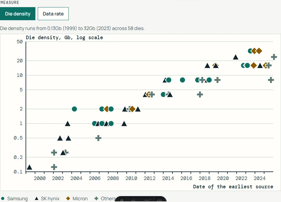
Three things are left to other pages. Dies and their history are in the DRAM Timeline. Part 4 covers the High Bandwidth Memory stack, which adds no new cell, and the Atlas takes one apart. Part 3 holds the cells that could follow DRAM, from capacitorless to ferroelectric, and the series page lists the rest.
Numbers here carry one of four tags. A datasheet value comes from a Micron datasheet for a named part and speed bin. Paper values are published measurements or models. Lecture values come from course slides or a tutorial and are used for an idea or a worked example, never as a product figure. Derived means arithmetic on numbers already given, shown in the text. Anything else is attributed to its source by name. None of the sources read is the DDR5 standard itself, JESD79-5, so every DDR5 timing in this part is attributed to Micron’s datasheet or papers.
The cell: one transistor, one capacitor
A DRAM cell is one access transistor and one storage capacitor, which is why it is called 1T1C. Its capacitor holds one bit as charge, and its transistor connects the capacitor to a bitline when a wordline switches it on (Lee and colleagues, HPCA 2015, paper). Everything else on a DRAM chip exists to write that charge, read it, and keep it from fading.
What the cell stores
A capacitor holds charge only for a while. According to a lecture from MIT, the capacitor leaks, so the cell must be refreshed periodically, on the order of milliseconds. The cell is also about 20 times smaller in area than an SRAM cell (lecture). Small size is why DRAM is dense, and the leak is why it needs refresh, which has its own section below.
Cell area is counted in units of F², where F is the smallest feature a process can draw. That unit is explained on the memory map. Most DRAM makers then used an 8F² cell, says a Micron tutorial at Hot Chips 16, and Micron’s 6F² cell, introduced in 256Mb production, cut array size by 25% at the same cell capacitance (lecture). Part 3 tells the story from 6F² to 4F². The High-NA EUV guide covers which DRAM nodes print with extreme ultraviolet (EUV) light. Samsung delivered its first EUV DRAM, on a first-generation 10nm-class node, in March 2020, SK hynix began mass production of 1a DRAM with EUV in July 2021, and Micron’s February 2025 release reports that its 1γ node uses EUV.
Why the bitline is the hard part
The cell is much smaller than the line it has to drive. The TL-DRAM paper (Lee and colleagues, HPCA 2013) puts a bitline’s capacitance at about 3.5 times the cell’s in its DDR3-class model (paper). When a row opens, the cell’s charge spreads over that larger capacitance and so the voltage on the line moves only a little. A UCSB lecture’s worked example puts that swing at about 250mV (lecture, a worked example and not a product figure).
This guide gives no capacitance in farads and no sense voltage for any product, since both would need a circuit paper first. The one number that carries the argument is the ratio.
The cell: one transistor, one capacitor
One transistor, one capacitor, and a sense amplifier
Schematic; the only number is the bit-line-to-cell ratio
Figure 2.1 draws the cell with its wordline, access transistor, capacitor and bitline, and puts a sense amplifier at the far end of the bitline. It is a schematic and carries one number, the ratio of about 3.5 (paper). Read it from the cell outward. It runs from a small capacitor, through a line several times its size, to an amplifier waiting at the end. The small swing therefore has to be amplified before anything can use it.
The sense amplifier
A sense amplifier is two cross-coupled inverters that act as a latch (Lee and colleagues, paper). Each bitline has one, and the UCSB lecture says a read needs one on every bitline (lecture). Across a row, the sense amplifiers make up the row buffer, the term the timing rules in the later sections refer to.
How the cell is built
The cell figure above is a circuit diagram. On a die, the same transistor and capacitor are cut into the silicon and built up above it one layer at a time, and Photolithography, Part 1 explains how each layer is printed. Samsung’s short course at the IEDM device conference names four process technologies that DRAM scaling rests on. Its list is patterning, the cell transistor, the transistors of the periphery and core, and the cell capacitor, and Part 3 reads the same course for where each one runs out of room. TechInsights lists the parts of the cell that makers keep as they scale it, from a 6F² cell and a buried-channel-array transistor (BCAT) on a saddle-shaped fin of silicon to a landing pad and plug for each storage node, an air-gap spacer beside each bitline, and a cylindrical or quasi-cylindrical capacitor built over the bitlines.
How the cell is built
A DRAM cell is stacked from the trench up
Two neighboring cells in cross-section; dashed parts come later
The figure stacks those parts from the trench up to the capacitor as a schematic with no dimensions. Each panel draws the same two cells with plain cylinders for capacitors, and a part that sits higher in the stack shows as a dashed outline until its own panel.
The wordline goes into the silicon
At the bottom is the transistor, whose gate is the wordline. Instead of lying on the surface, the wordline is set into a trench etched in the silicon, so the channel runs down one side of the trench, under it and up the other. That recessed channel and buried gate make the channel longer than the surface it spans, which is why makers adopted the BCAT to hold off short-channel effects (a simulation study in Micromachines, paper).
The baseline process of an IEDM paper on cell transistors builds the buried gate from titanium nitride deposited into the trench and recessed by a dry etch-back (paper). The paper names n+ polysilicon over titanium nitride the dual-workfunction gate and calls it the industry standard. Its polysilicon suppresses gate-induced drain leakage at the expense of gate resistance, which is why the paper proposes replacing it (paper).
Contacts and the bitline
Bitlines run above the buried wordlines. Two neighboring cells share one bitline through a single bitline contact, though each has its own storage node and wordline (DRAMScope, paper). Each storage node still needs its own path up past the bitlines, and this page reads the plug and landing pad in TechInsights’ list as that path.
The capacitor goes on top
The capacitor sits on top of the array, over the bitlines, in a layout TechInsights calls capacitor on bitline. Its insulator is a high-k film. Samsung’s 18nm DRAM has a honeycomb-type capacitor, and in it TechInsights found an ultra-thin double layer of zirconium oxide and aluminum zirconium oxide that was even from top to bottom. In the 20nm-class generation before it, the film had been thicker at the top than at the bottom.
The transistors around the array
Sense amplifiers and the rest of the periphery need transistors of their own, and the short course lists them as a separate technology. Micron says its 1γ node uses next-generation high-k metal gate CMOS to improve transistor performance and circuit area. Photolithography, Part 3 covers the EUV layers that came in over the same generations.
The read cycle: share, sense, restore
A read on one bitline takes four steps, namely precharge, charge sharing, sensing and restore. Timing parameters on a datasheet are points on that curve, so the curve comes first.
Precharge and charge sharing
Lee and colleagues walk the access in states (paper). Before the access, the bitline rests at half of VDD (the supply voltage). After ACTIVATE the wordline rises and the cell drives its charge onto the bitline, so the two settle at half of VDD plus a small difference. That step is charge sharing. A Penn lecture explains the midpoint start. Precharging to VDD/2 keeps the shared charge from swinging the line across it (lecture).
Sense and restore: a read is also a write
Next, the sense amplifier magnifies the small difference and drives the bitline to VDD. That also pushes charge back into the cell (paper). Raising a row’s wordline connects every capacitor in the row to its bitline, and the row buffer then reads out the charge, which destroys the data in the cells, and immediately writes the charge back (Kim and colleagues, ISCA 2014, paper).
So a read ends with the cell restored. Restoring matters beyond reads, because refresh will reuse the step.
Where tRCD, tRAS and tRP fall
In Lee and colleagues’ paper the timing parameters are the times to reach points on that curve after ACTIVATE. tRCD (the row-to-column delay) is the time to the middle of sensing, with the bitline near three-quarters of VDD, after which a read or write can be issued. tRAS is the time to full restore at VDD. tRP is the precharge. The wordline goes down, then the sense amplifier switches off, and the bitline returns to half of VDD. tWR adds time after a write (paper). That paper’s DDR3-1600 values are tRCD 13.75ns, tRAS 35ns, tRP 13.75ns and tWR 15ns (paper).
An access to a rank has three steps. ACTIVATE moves the row into the bank’s row buffer, then a read or write takes columns from that buffer, and PRECHARGE closes the row (Kim and colleagues, paper). The row cycle time (tRC) is the delay between ACTIVATEs to the same bank, and Kim and colleagues give it as about 50ns typically (paper). That caps how fast one row can be opened and closed. At ISCA 2025 the Rambus tutorial draws the same access in five steps, with tRCD, tRAS, tRP and tRC marked.
The read cycle: share, sense, restore
Where tRCD, tRAS and tRP fall on one access
Schematic after Lee and colleagues; time axis not to scale
Figure 2.3 draws that curve as a schematic after Lee and colleagues. The time axis is not to scale and so the intervals show order and say nothing of duration. Beneath it, a strip carries the DDR3-1600 values as real numbers. Most timings in the sections that follow are either a point on this curve or a rule about sharing the chip between banks. Refresh timings are the exception, and they get their own section.
Rows, banks, groups and ranks
Between a processor and one cell lie a memory controller, channel, module, ranks, dies, bank groups, banks, mats and finally cells (Rambus tutorial, lecture). Each level has its own timing rule, and the rules in the timing sections below are written against these names.
The row buffer
An ACTIVATE moves a row into the sense amplifiers, which are the row buffer. Reads and writes then take columns from that buffer. A request to the row that is already open is a hit and needs no new ACTIVATE. Asking for a different row in the same bank is a conflict, and it costs a precharge and a new activate (Mutlu’s ACACES lecture, lecture).
Row size depends on what is counted. In one die, one activation senses 1KB to 2KB of cells (Rambus tutorial, lecture). Kim and colleagues’ example of an 8KB row is a rank-level row, in a 2GB rank of eight banks of 32K rows (paper). The two sizes measure different things, and neither should be averaged with the other.
Banks and subarrays
A bank can open only one row at a time, but it does so independently of the other banks. Several banks therefore give parallelism, because different banks can serve requests at once (Kim and colleagues, 2014, paper, and the Rambus tutorial). Inside a bank the cells are not one array. The SALP paper (Kim and colleagues, ISCA 2012) says a bank is made of subarrays, because one long bitline would be slow. Each subarray has a local row buffer, and the subarrays share a row-address decoder and global bitlines to a global row buffer (paper).
The Rambus tutorial draws a bank below that as an array of mats, with wordline drivers beside each mat and decoders at the bank’s edges. Mat counts and sizes differ by vendor and generation, it says (lecture).
Bank groups
A bank group works independently but shares timing control, data lines and command lines among its banks, according to the Rambus tutorial (lecture). That sharing is why accesses inside one group wait longer than accesses across groups, and the timing section below gives the rules.
Bank count depends on the generation, the density and the chip width. DDR4 has 16 banks, as 4 groups of 4, for x4 and x8 devices, and 8 banks, as 2 groups of 4, for x16 devices (Micron DDR4 datasheet, datasheet). A DDR5 die of 8Gb has 16 banks for x4 and x8, as 8 groups of 2, or 8 banks for x16, as 4 groups of 2. At 16Gb and above the banks double, to 32 for x4 and x8, as 8 groups of 4, or 16 for x16, as 4 groups of 4 (Micron DDR5 datasheet, datasheet). JEDEC’s DDR5 announcement says 32 banks from 16. Reading that as the 16Gb case is an inference, so the datasheet’s count by density is the one to use.
At 16Gb and above, DDR5 has twice DDR4’s groups with the same four banks in each. Doubling the groups lets more pages stay open and raises the odds of a page hit, says Micron’s white paper on DDR5’s new features.
Ranks, channels and DDR5 sub-channels
One chip has a small capacity and a narrow bus, so chips are ganged into a rank, typically a 64-bit bus (Kim and colleagues, paper). Chips come in x4, x8 and x16 widths. A Synopsys white paper says a standard DDR channel is 64 bits wide and that DIMMs on one channel share command, address and data wires (white paper).
DDR5 changes the channel. JEDEC’s announcement says DDR5 doubles the burst length to 16 and that the DIMM carries two fully independent 40-bit sub-channels. According to Micron’s DDR5 white paper, each is 32 bits plus ECC, and that with a burst length of 16 one burst fetches a 64-byte cache line from only one sub-channel, which is half the DIMM. It adds that this turns an 8-channel system into a 16-channel one for concurrency.
Rows, banks, groups and ranks
From channel to row, and the DDR5 bank layout
Left nesting is a schematic; right is DDR5 16Gb, 8 groups of 4
Figure 2.4 has two panels. The left panel nests the levels from channel to row, as a schematic. The right panel draws the DDR5 16Gb bank layout, eight groups of four, with one group highlighted. Its only numbers are the 64-bit rank, the eight-by-four layout and the two 32-bit sub-channels (40 bits with ECC), and each carries its tag.
Refresh is a row operation
Refresh is the read cycle with the column output removed, which follows from the restore step in the read cycle. Part 3 holds the cost-of-refresh argument, and this part stays with the mechanism.
A refresh is a read without the output
A Berkeley lecture describes a refresh as a read with no column output. The row is moved onto its sense amplifiers, each amplifier boosts the value and drives it back into the storage cell, and nothing leaves the chip (lecture). It is the restore step from the last section, and the reason the read cycle came first. An ordinary read also refreshes its row as a side effect (lecture).
The window and the command count
A cell must be refreshed or accessed at least once within its retention period. Bhati and colleagues (IEEE Transactions on Computers, 2016) say most commodity DRAM has a 32 or 64ms refresh window, which shortens with temperature, and that the controller issues auto-refresh commands at an interval called tREFI across that window. A DDR3 device has a tREFI of 7.8µs and a 64ms window, so 8,192 commands (paper). A Micron Hot Chips tutorial shows the arithmetic. 64ms over 8K commands is 7.8125µs, and over 4K commands it would be 15.625µs (lecture).
Window and interval differ by standard and temperature. Micron’s DDR4 datasheet requires 8,192 commands in 64ms up to 85°C, one every 7.8125µs, and in 32ms above 85°C up to 95°C (datasheet). The DDR5 datasheet requires 8,192 commands within 32ms from 0°C to 85°C, which is one every 3.9µs, and within 16ms from 85°C to 95°C, which is one every 1.95µs. Micron’s 16Gb DDR5 die datasheet gives the same windows and intervals (datasheet).
Each command refreshes a few rows in each bank, and the chip keeps the row counter (Bhati and colleagues, paper). DRAM vendors refresh several rows with one command to cut the volume of refresh traffic (Stuecheli and colleagues, MICRO 2010, paper).
All-bank and per-bank refresh
Commodity DDR uses all-bank refresh. One command refreshes some rows in every bank of a rank and leaves every bank unavailable until it finishes (Chang and colleagues, HPCA 2014, paper). LPDDR also offers per-bank refresh, so one bank refreshes while the others serve requests. Bhati and colleagues add that the command cannot name the bank, because the device keeps a bank counter and steps it from bank 0 on each command (paper).
Refresh has two modes, auto-refresh when the device is busy and self-refresh when it is idle, to save power. Banks must be precharged before an auto-refresh, and normal operation resumes only after the refresh cycle time (tRFC) has passed (Bhati and colleagues, paper).
What a DDR5 refresh command costs
In normal mode, Micron’s DDR5 datasheet lists tRFC for an all-bank command as 195, 295, 410 and 410ns for 8, 16, 24 and 32Gb dies. In fine-granularity mode the all-bank time, tRFC2, is 130, 160, 220 and 220ns for the same four sizes. Same-bank refresh, called REFsb, takes 115, 130, 190 and 190ns for those sizes. An ACTIVATE to a different bank can follow after 30ns, while the refreshed banks wait the full same-bank refresh time (datasheet).
Micron’s white paper explains why REFsb exists. It targets the same bank in every bank group, so only that bank in each group must be idle while the rest stay usable. For a 16Gb part the white paper gives 130ns for REFsb against 295ns for an all-bank refresh in normal mode, and says REFsb works only in fine-granularity mode, where the datasheet’s all-bank time is 160ns. Like for like, that is 130ns against 160ns (derived).
Read these numbers within one generation. DDR4’s all-bank tRFC rises from 160ns at 2Gb to 550ns at 16Gb (datasheet), and DDR4 at 8Gb is 350ns, against 195ns for DDR5 at 8Gb. DDR3 shows the same rise with density, from 90ns at 512Mb to 350ns at 8Gb (Stuecheli and colleagues, MICRO 2010, paper). The growth comes with density inside a generation and not from one generation to the next. How tRFC grows with density, and what could cut the cost, is in Part 3.
Refresh is a row operation
One DDR5 16Gb refresh: all-bank against same-bank
Command duration to scale; same-bank commands come more often
Figure 2.5 draws the two commands on one nanosecond scale. In normal mode the all-bank command blocks every bank for 295ns, and the same-bank command blocks one bank in each group for 130ns in fine-granularity mode, where the all-bank command takes 160ns, while the other banks stay usable. Same-bank commands do not come once per 3.9µs interval: in fine-granularity mode each bank must be refreshed every 1.95µs on average, according to the Micron white paper, so they come more often. Turning either into a share of time is arithmetic, and Part 3 owns that argument.
What the DDR timing numbers measure
A DIMM label such as 22-22-22 and a datasheet row such as tRCD 16.000ns count the same intervals, one in clocks and one in nanoseconds. CL (the CAS latency, tCL) is the delay the TL-DRAM paper adds after tRCD for the peripherals and input/output circuitry, so a first access takes tRCD + tCL + tBL, where tBL is the bus time (paper). That puts CL after the row is open and not on the bitline curve. The other two label numbers are tRCD and tRP counted in clocks, and the conversion to nanoseconds follows.
Timing inside one bank
tRCD, tRAS and tRP are the intervals from the read cycle, and tRC is tRAS plus tRP. In Micron’s DDR5 datasheet, the DDR5-4800B bin is CL-nRCD-nRP of 40-39-39, with tRCD and tRP of 16.000ns, tRAS of at least 32.000ns and tRC of 48.000ns. For the AN bin the datasheet gives 34-34-34, with tRCD and tRP of 14.166ns (datasheet).
A clock-count label converts to nanoseconds by multiplying by the clock period, and the datasheet rounds the clock count up from its nanosecond minimum, so the product can come out a little above the listed time. In Micron’s DDR4 datasheet, the DDR4-3200 bins are 20-20-20, 22-22-22 and 24-24-24 at a 0.625ns clock. So the 22-22-22 bin has a tRCD of 22 times 0.625ns, which is 13.75ns (derived from the datasheet). This belongs to the bin and not to the generation. Another DDR4 bin, or another DDR5 bin, gives a different tRCD, and any quoted figure should name the bin.
Timing between banks: tRRD and tFAW
A row stays open until PRECHARGE, and a bank must be precharged before a different row opens in it. ACTIVATEs to different banks are spaced as well. DDR5 uses a long spacing, tRRD_L, within a bank group and a short one, tRRD_S, across groups, and it allows no more than four ACTIVATEs inside a window called tFAW (datasheet).
At DDR5-3200 the datasheet gives tRRD_L as the larger of 8 clocks and 5ns, tRRD_S as 8 clocks, and tFAW as the larger of 32 clocks and 20ns for 1KB pages, or the larger of 40 clocks and 25ns for 2KB pages (datasheet). Both the clock count and the nanosecond floor apply, and the larger one wins.
Timing within a group: tCCD_L and tCCD_S
Column accesses follow the same split. Back-to-back column commands in the same bank group wait the long interval, tCCD_L, and commands across groups wait the short one, tCCD_S. Micron’s white paper on DDR5’s new features calls tCCD_L, tWTR_L and tRRD_L the long timings, and their _S forms the short ones. It adds that tCCD_L can be nearly double tCCD_S. The Rambus tutorial gives the reason, which is the sharing from the last section. While one bank in a group is being read or written, the others in that group cannot be (lecture).
The core stays near 14 to 16ns while the pins triple
tRCD is 13.75ns for DDR3-1600 (paper), 13.75ns for the DDR4-3200 22-22-22 bin (derived from the datasheet) and 16.000ns for DDR5-4800B (datasheet). Across those three the data rate goes from 1,600 to 3,200 to 4,800MT/s. Array latency stays near 14 to 16ns while the pin rate triples (derived).
Pins get faster because each access moves more data, while the array is no quicker. Core timing is not scaling while burst length keeps rising with clock speed, says the Rambus tutorial. One read per row activation then uses under 10% of the data bus, and repeated reads from an open row use under 50% at DDR5-8000 (lecture, where the DDR5-8000 is the tutorial’s own figure and not a datasheet’s). Prefetch is how the array keeps up. DDR4’s datasheet describes an 8n prefetch, one 8n-bit transfer over four core clocks matched by eight half-clock transfers at the pins (datasheet). For DDR5 the datasheet describes a 16n prefetch, one 16n-bit transfer over eight core clocks matched by sixteen half-clock transfers (datasheet).
What the DDR timing numbers measure
Pin rate triples, tRCD stays near 14 to 16ns
Three generations; each point tagged by source
Figure 2.6 puts the three generations on one axis. The top panel is the data rate and the bottom panel is tRCD, with three points each and the source of each point tagged. Its small inset marks tRCD on the curve from Figure 2.3, so the two figures share a vocabulary.
Same cell, three buses
This section rests on vendor, standards-body press and secondary sources. These are white papers, press releases, slide decks and a tutorial, with one GDDR6 datasheet. None of them is a standard text, and the section says where each statement comes from.
What stays the same
A Synopsys white paper says the three JEDEC DRAM categories, standard DDR, mobile LPDDR and graphics GDDR, use the same DRAM array for storage, with a capacitor as the basic storage element. They differ in data width and rate, host connection, electrical specification, pin termination and power states. It says LPDDR has a memory array identical to standard DDR’s, with channels typically 16 or 32 bits wide against 64 bits for DDR (white paper).
DDR came first, says the Rambus tutorial. Early phones used standard DDR DRAM, growing volumes later justified the LPDDR variant, and GPUs followed the same path from DDR to GDDR2 and the later GDDR generations (lecture). So the cell, the read cycle and the refresh described above sit behind all three. Mostly the bus in front of the array changes.
DIMM, phone, graphics
A DDR5 DIMM has two independent 32-bit sub-channels, 40 bits each with ECC, and a 16n prefetch, as the sections above give. LPDDR4 is described in a Micron slide deck at the JEDEC Mobile Forum. It has a 2KB page, two independent x16 channels, 8 banks per channel (16 per die), and a 16n prefetch of 32 bytes per column command (slide deck).
LPDDR5 is in JEDEC’s announcement. It targets 6,400MT/s against 3,200MT/s for LPDDR4 and offers programmable bank organization of 8 banks, 4 bank groups of 4 banks, or 16 banks. An arXiv study says an LPDDR4 channel always has 8 banks, while LPDDR5 runs 16 banks by default up to 3,200MT/s, 4 bank groups at higher rates, or an 8-bank mode with a 32n prefetch. The 16-bank and bank-group modes use a 16n prefetch (study).
Micron’s GDDR6 datasheet describes two independent x16 channels, 16 banks in 4 bank groups, and a 16n prefetch of 256 bits per array access (datasheet). Synopsys’s white paper gives GDDR6 up to 16Gb/s per pin, and says GDDR5X differed from GDDR5 chiefly by a 16n prefetch in place of 8n (white paper). JEDEC’s GDDR7 announcement says GDDR7 uses PAM3, which sends 3 bits over 2 cycles using three signal levels, and that independent channels double from 2 in GDDR6 to 4.
One array cycle, a different pin rate
Prefetch is the bridge between the array and the pins. A Rambus technical article on GDDR6 explains that each of the two channels reads or writes 256 bits, or 32 bytes, per access. Because of the 16n prefetch, the same internal array cycle of 1ns equals a 16Gb/s pin rate (article). The DDR4 to DDR5 step looks like the same move, from an 8n prefetch to 16n: a wider prefetch lets an array cycle of the same length feed a faster pin. That reading is an inference from the two prefetch figures, not a statement in either datasheet.
Refresh differs by part. GDDR6 auto refresh is 32ms with 16K cycles, with per-bank and per-2-bank options (datasheet). LPDDR’s per-bank refresh is in the refresh section above.
Same cell, three buses
One array, three buses in front of it
Shaded by evidence; channels per DIMM for DDR5, per die for the others
Figure 2.7 draws the shared array once at the top and the three buses beneath it as a grid of channel width, channels (per DIMM for DDR5, per die for the others), prefetch and banks. Each cell is shaded by the kind of source behind it, datasheet, press release or secondary, and GDDR7 appears as a single row, PAM3 and four channels.
Part 3 starts from this cell and asks what could follow 1T1C.
Sources
Primary is the original paper, standard or datasheet. Secondary is a review, a vendor summary or a news report. Measured is my own test data.
Show all 36 sources, 22 primary
- PrimaryStuecheli et al. 2010 Elastic Refresh: techniques to mitigate refresh penalties in high density memoryMICRO 2010 (University of Texas at Austin), 2010
- PrimaryKim et al. 2012 A Case for Exploiting Subarray-Level Parallelism (SALP) in DRAM (ISCA)ISCA 2012 (Carnegie Mellon University), 2012
- PrimaryTiered-Latency DRAM: A Low Latency and Low Cost DRAM ArchitectureHPCA 2013, 2013
- PrimaryChang et al. 2014 Improving DRAM Performance by Parallelizing Refreshes with Accesses (HPCA)HPCA 2014 (Carnegie Mellon University, Intel Labs), 2014
- PrimaryKim et al. 2014 Flipping Bits in Memory Without Accessing Them: DRAM disturbance errors (ISCA)ISCA 2014 (Carnegie Mellon University, Intel Labs), 2014
- PrimaryLee et al. 2015 Adaptive-Latency DRAM: Optimizing DRAM Timing for the Common-Case (HPCA)HPCA 2015 (Carnegie Mellon University), 2015
- PrimaryDRAM refresh mechanisms, penalties, and trade-offsIEEE Transactions on Computers (University of Maryland), 2016
- PrimaryMicron 4Gb x4, x8, x16 DDR4 SDRAM data sheet (Rev. J, 2017)Micron Technology (copy hosted by xonstorage), 2017
- PrimaryJEDEC Publishes New DDR5 StandardJEDEC, 2020
- PrimarySamsung Announces Industry’s First EUV DRAM with Shipment of First Million ModulesSamsung, 2020
- PrimaryMicron DDR5 SDRAM: product core data sheetMicron Technology (copy hosted by Farnell), 2022
- PrimaryMicron 16Gb DDR5 SDRAM Die Rev A: data sheet addendumMicron Technology (copy hosted by Farnell; micron.com download is login-gated), 2023
- PrimaryA Workfunction Engineered Middle-Silicon-TiN Gate (MSTG) Cell Transistor in 16Gbit DRAM for High Scalability and Long Data Retentioniedm23.mapyourshow.com
- PrimaryDRAMScope: Uncovering DRAM Microarchitecture and Characteristics by Issuing Memory Commandsarxiv.org
- PrimaryIntroducing Micron DDR5 SDRAM: More Than a Generational Update (white paper)Micron Technology
- PrimaryJEDEC Publishes GDDR7 Graphics Memory StandardJEDEC
- PrimaryJEDEC Updates Standard for Low Power Memory Devices: LPDDR5JEDEC
- PrimaryMicron 1γ (1-gamma) DDR5: product briefMicron Technology
- PrimaryMicron Announces Shipment of 1γ (1-gamma) DRAM: Pioneering Memory Technology Advancements for Future Compute NeedsMicron Technology
- PrimaryMicron DDR5 SDRAM: New Features (white paper, Rooney and Koyle)Micron Technology
- PrimaryMicron GDDR6 SGRAM MT61K256M32 data sheet (8Gb, 2 channels x16)Micron Technology (copy hosted by micron-electronic.com)
- PrimarySK hynix Starts Mass Production of 1anm DRAM Using EUV EquipmentSK hynix
- SecondaryPawlowski (Micron) 2004 Memory Performance Tutorial, Hot Chips 16Hot Chips 16 (Micron Technology), 2004
- SecondaryMutlu 2013 Scalable Many-Core Memory Systems, Lecture 1: DRAM Basics and DRAM Scaling (ACACES, after lecture)ACACES 2013 (Onur Mutlu, Carnegie Mellon University), 2013
- SecondarySkinner (Micron) 2013 LPDDR4 architectural approach, JEDEC Mobile ForumJEDEC Mobile Forum (Micron Technology), 2013
- SecondaryUnveiling the Real Performance of LPDDR5 Memories (arXiv 2209.14756)arXiv, 2022
- SecondaryMIT 6.004 Fall 2023 lecture: The Memory Hierarchy (SRAM and DRAM cells)MIT, 2023
- SecondaryUCSB ECE 122A Lecture 16 (Banerjee): memory cells, 1T DRAM charge redistributionUniversity of California, Santa Barbara, 2023
- SecondaryEvolution of Memory Technologies for Advanced Nodes via the 3rd DimensionIEDM 2024 short course, 2024
- SecondaryPenn ESE 3700 Lecture 19: RAM Core and Periphery (1T DRAM cell, charge sharing)University of Pennsylvania, 2024
- SecondaryCS 294-4 Lecture 2: DRAMUC Berkeley
- SecondaryDRAM Scaling Trend and Beyondtechinsights.com
- SecondaryGoing Beyond GPUs with GDDR6 — Rambus Technical ArticleChipEstimate
- SecondarySamsung 18 nm DRAM cell integration: QPT and higher uniformed capacitor high-k dielectricstechinsights.com
- SecondaryScaling DRAM Technology to Meet Future Demands: Challenges and Opportunities (ISCA 2025 Tutorial)Rambus
- SecondaryWhich DDR SDRAM Memory to Use and When (Synopsys white paper)Synopsys